Detailed description, Dual charge-pump voltage converter – Rainbow Electronics MAX13175E User Manual
Page 22
MAX13171E/MAX13173E/MAX13175E
Multiprotocol, Pin-Selectable
Data Interface Chipset
22
______________________________________________________________________________________
R1A
R2A R2B R3A R3B R4A R4B R5A R5B R6A R6B
M2 M1 M0
R1B
DCE/DTE
LATCH
MAX13175E
V
L
V
CC
V
DD
V
EE
GND
V
EE
EP
R1C
R2C
R3C
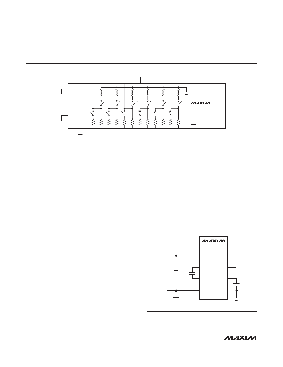
Figure 14. MAX13175E Block Diagram
Detailed Description
The MAX13171E/MAX13173E/MAX13175E form a com-
plete pin-selectable DTE or DCE interface port that
supports the V.28 (RS-232), V.10/V.11 (RS-449/V.36,
RS-530, RS-530A, X.21), and V.35 protocols. The
MAX13171E transceivers carry the high-speed clock
and data signals, while the MAX13173E transceivers
carry serial-interface control signaling. The MAX13171E
can be terminated by the MAX13175E pin-selectable
resistor termination network, or by a discrete termina-
tion network. The MAX13171E/MAX13173E feature a
low supply current, no-cable mode, true fail-safe opera-
tion, and thermal-shutdown circuitry. Thermal shutdown
protects the drivers against excessive power dissipa-
tion. When activated, the thermal-shutdown circuitry
places the driver and receiver outputs into a high-
impedance state.
The MAX13171E is a three-driver/three-receiver, multi-
protocol transceiver that operates from a single
+3.135V to +5.5V supply. The MAX13173E is a five-dri-
ver/five-receiver multiprotocol transceiver that operates
from a single +3.135V to +5.5V supply. The
MAX13175E contains six pin-selectable multiprotocol
cable termination networks (Figure 14). Each network is
capable of terminating V.11 (RS-422, RS-530, RS-530A,
RS-449, V.36 and X.21) with a 100Ω differential load,
V.35 with a T-network load, or V.28 (RS-232) and V.10
(RS-423) with an open-circuit load for use with trans-
ceivers having on-chip termination. The terminations
and protocols are pin selectable. The MAX13175E
replaces discrete resistor termination networks and
expensive relays required for multiprotocol termination,
saving space and cost.
Dual Charge-Pump Voltage Converter
The MAX13171E/MAX13173E have internal-regulated
dual charge pumps that provide positive and negative
output voltages from a single supply. The charge pump
operates in discontinuous mode. If the output voltage is
less than the regulated voltage, the charge pump is
enabled. If the output voltage exceeds the regulated
voltage, the charge pump is disabled. Each charge
pump requires flying capacitors (C1, C2), and reservoir
capacitors (C3, C5), to generate the V
DD
and V
EE
sup-
plies. Figure 15 shows the charge-pump connections.
C2-
V
EE
C2+
MAX13171E
MAX13173E
GND
C1-
+3.135V
TO +5.5V
V
CC
V
DD
C1+
C1
1µF
C5
4.7µF
C2
1µF
C3
4.7µF
C4
4.7µF
Figure 15. Charge Pump