Rainbow Electronics MAX13175E User Manual
Page 16
MAX13171E/MAX13173E/MAX13175E
Multiprotocol, Pin-Selectable
Data Interface Chipset
16
______________________________________________________________________________________
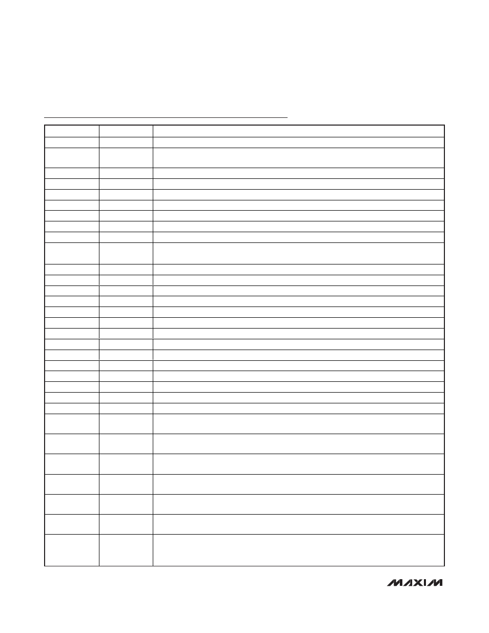
MAX13171E Pin Description
PIN
NAME
FUNCTION
1, 2, 6, 30, 31
N.C.
No Connection. Not internally connected.
3, 16
V
CC
Device Supply Voltage. Bypass V
CC
with a 4.7µF capacitor to ground as close as possible to
pin 3.
4
T1IN
Transmitter 1 Logic Input
5
T2IN
Transmitter 2 Logic Input
7
T3IN
Transmitter 3 Logic Input
8
R1OUT
Receiver 1 Logic Output with Internal Pullup to V
L
9
R2OUT
Receiver 2 Logic Output with Internal Pullup to V
L
10
R3OUT
Receiver 3 Logic Output with Internal Pullup to V
L
11
M0
Mode-Select 0 Input with Internal Pullup to V
L
12
V
L
Logic-Supply Reference Input. V
L
determines the voltage level of the logic interface. Bypass V
L
with a 0.1µF capacitor to ground as close as possible to the device.
13
M1
Mode-Select 1 Input with Internal Pullup to V
L
14
M2
Mode-Select 2 Input with Internal Pullup to V
L
15
DCE/DTE
DCE/DTE Mode-Select Input with Internal Pullup to V
L
17
R3INB
Receiver 3 Noninverting Input
18
R3INA
Receiver 3 Inverting Input
19, 24, 29, 35
GND
Ground
20
R2INB
Receiver 2 Noninverting Input
21
R2INA
Receiver 2 Inverting Input
22
T3OUTB/R1INB
Transmitter 3 Noninverting Output/Receiver 1 Noninverting Input
23
T3OUTA/R1INA
Transmitter 3 Inverting Output/Receiver 1 Inverting Input
25
T2OUTB
Transmitter 2 Noninverting Output
26
T2OUTA
Transmitter 2 Inverting Output
27
T1OUTB
Transmitter 1 Noninverting Output
28
T1OUTA
Transmitter 1 Inverting Output
32
V
EE
Charge-Pump Negative Supply Output. Connect a 4.7µF ceramic capacitor from V
EE
to ground
as close as possible to the device.
33
C2-
V
EE
Charge-Pump Flying-Capacitor Negative Terminal. Connect a 1µF ceramic capacitor
between C2+ and C2-.
34
C2+
V
EE
Charge-Pump Flying-Capacitor Positive Terminal. Connect a 1µF ceramic capacitor
between C2+ and C2-.
36
C1-
V
DD
Charge-Pump Flying-Capacitor Negative Terminal. Connect a 1µF ceramic capacitor
between C1+ and C1-.
37
C1+
V
DD
Charge-Pump Flying-Capacitor Positive Terminal. Connect a 1µF ceramic capacitor
between C1+ and C1-.
38
V
DD
Charge-Pump Positive-Supply Output. Connect a 4.7µF ceramic capacitor from V
DD
to ground
as close as possible to the device.
—
EP
Exposed Pad. Internally connected to V
EE
. Connect to a large V
EE
plane to maximize thermal
performance. Not intended as an electrical connection point. Do not share the same plane as
the MAX13173E.