Rainbow Electronics MAX13175E User Manual
Page 29
MAX13171E/MAX13173E/MAX13175E
Multiprotocol, Pin-Selectable
Data Interface Chipset
______________________________________________________________________________________
29
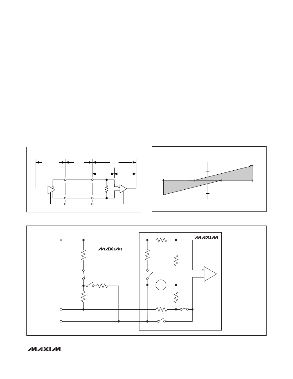
V.11 (RS-422) Interface
As shown in Figure 21, the V.11 protocol is a fully bal-
anced differential interface. The V.11 driver generates a
minimum of ±2V between nodes A and B when a 100Ω
(min) resistance is present at the load. The V.11 receiver
is sensitive to differential signals of ±200mV at receiver
inputs A’ and B’. The V.11 receiver input must comply
with the impedance curve of Figure 22 and reject com-
mon-mode signals developed across the cable (refer-
enced from C to C’ in Figure 21) of up to ±7V.
The MAX13171E/MAX13173E V.11 mode receivers
have a differential threshold between -50mV and
-200mV to ensure that the receiver has fail-safe opera-
tion (see the
Fail-Safe
section.) To aid in rejecting sys-
tem noise, the MAX13171E/MAX13173E V.11 receivers
have a typical hysteresis of 15mV. Switch S3 in Figure
23 is open in V.11 mode to disable the V.28 5kΩ termi-
nation at the inverting receiver input. Because the con-
trol signals are slow (60kbps), 100Ω termination
resistance is generally not required for the MAX13173E.
For high-speed data transmission, the V.11 specifica-
tion recommends terminating the cable at the receiver
with a 100Ω resistor. This resistor, although not
required, prevents reflections from corrupting transmit-
ted data. In Figure 23, the MAX13175E is used to termi-
nate the V.11 receiver. Internal to the MAX13175E, S1 is
closed and S2 is open to present a 100Ω minimum dif-
ferential resistance. The MAX13171E’s internal V.28 ter-
mination is disabled by opening S3.
R6
11kΩ
R8
5kΩ
R3
127Ω
R2
52Ω
R1
52Ω
A′
B′
C′
A
B
GND
R5
55kΩ
1.4V
R7
11kΩ
R4
55kΩ
MAX13175E
MAX13171E
S3
S1
RECEIVER
S2
S2
+
-
S1
Figure 23. V.11 Termination and Internal Resistance Networks
100Ω
MIN
A′
B′
C′
A
B
C
GENERATOR
BALANCED
INTERCONNECTING
CABLE
CABLE
TERMINATION
RECEIVER
LOAD
Figure 21. Typical V.11 Interface
-3.25mA
+3.25mA
-10V
+10V
-3V
+3V
V
Z
I
Z
Figure 22. Receiver Input Impedance