Dc electrical characteristics (continued) – Rainbow Electronics MAX5489 User Manual
Page 4
MAX5487/MAX5488/MAX5489
Dual, 256-Tap, Nonvolatile, SPI-Interface,
Linear-Taper Digital Potentiometers
4
_______________________________________________________________________________________
Note 1: All devices are production tested at T
A
= +25°C and are guaranteed by design and characterization for -40°C < T
A
< +85°C.
Note 2: DNL and INL are measured with the potentiometer configured as a voltage-divider with H_ = V
DD
and L_ = 0. The wiper terminal
is unloaded and measured with an ideal voltmeter.
Note 3: DNL and INL are measured with the potentiometer configured as a variable resistor. H_ is unconnected and L_ = 0. For V
DD
=
+5V, the wiper terminal is driven with a source current of 400µA for the 10k
Ω configuration, 80µA for the 50kΩ configuration,
and 40µA for the 100k
Ω configuration. For V
DD
= +3V, the wiper terminal is driven with a source current of 200µA for the 10k
Ω
configuration, 40µA for the 50k
Ω configuration, and 20µA for the 100kΩ configuration.
Note 4: The wiper resistance is the worst value measured by injecting the currents given in Note 3 into W_ with L_ = GND. R
W
=
(V
W
- V
H
) / I
W
.
Note 5: The device draws higher supply current when the digital inputs are driven with voltages between (V
DD
- 0.5V) and (GND +
0.5V). See Supply Current vs. Digital Input Voltage in the Typical Operating Characteristics section.
Note 6: Wiper at midscale with a 10pF load.
Note 7: Wiper-settling time is the worst-case 0-to-50% rise time, measured between tap 0 and tap 127. H_ = V
DD
, L_ = GND, and
the wiper terminal is unloaded and measured with a 10pF oscilloscope probe (see Tap-to-Tap Switching Transient in the
Typical Operating Characteristics section).
Note 8: Digital timing is guaranteed by design and characterization, and is not production tested.
DC ELECTRICAL CHARACTERISTICS (continued)
(V
DD
= +2.7V to +5.25V, V
H
= V
DD
, V
L
= GND, T
A
= -40
°C to +85°C, unless otherwise noted. Typical values are at V
DD
= +5.0V,
T
A
= +25
°C, unless otherwise noted.) (Note 1)
PARAMETER
SYMBOL
CONDITIONS
MIN
TYP
MAX
UNITS
POWER SUPPLIES
Power-Supply Voltage
V
DD
2.70
5.25
V
Supply Current
I
DD
During write cycle only, digital inputs =
V
DD
or GND
400
µA
Standby Current
Digital inputs = V
DD
or GND, T
A
= +25°C
0.5
1
µA
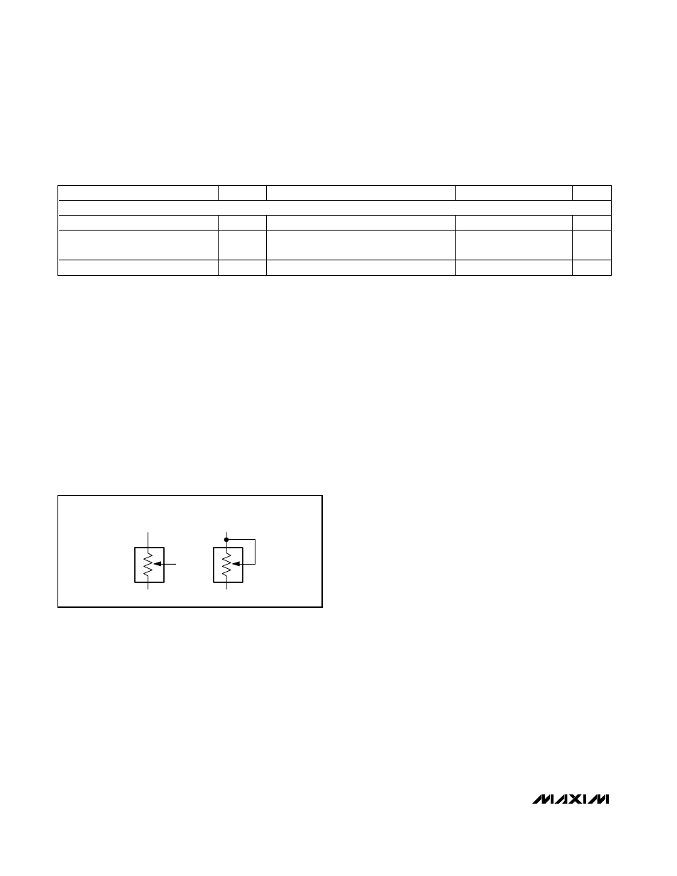
H
L
W
VOLTAGE-DIVIDER
CONFIGURATION
VARIABLE-RESISTOR
CONFIGURATION
H
L
Figure 1. Voltage-Divider/Variable-Resistor Configurations