Rainbow Electronics MAX7358 User Manual
Page 6
MAX7356/MAX7357/MAX7358
1-to-8 I
2
C Bus Switches/Multiplexers with Bus
Lock-Up Detection, Isolation, and Notification
6
_______________________________________________________________________________________
TIMING CHARACTERISTICS (FAST-MODE) (Figures 1, 2, 3) (continued)
(V
DD
= 2.3V to 5.5V, T
A
= -40°C to +85°C, unless otherwise noted.) (Notes 2, 6)
Note 2: All devices are 100% production tested at T
A
= +25°C. Specifications are over -40°C to +85°C and are guaranteed by
design.
Note 3: Subscript SW refers to all SC_ and SD_ pins.
Note 4: V
SWin
= Switch input voltage; I
SWout
= Current between SD_ and SDA or SC_ and SCL. See Figure 4.
Note 5: V
I
= V
SD_
or V
SC_
.
Note 6: All timing is measured using 20% and 80% levels, unless otherwise noted.
Note 7: Pass gate propagation delay is calculated from the 20
Ω typical R
ON
and the 15pF load capacitance.
Note 8: A device must internally provide a hold time of at least 300ns for the SDA signal (referred to the V
IH(min)
of the SCL signed)
to bridge the undefined region of the falling edge of SCL.
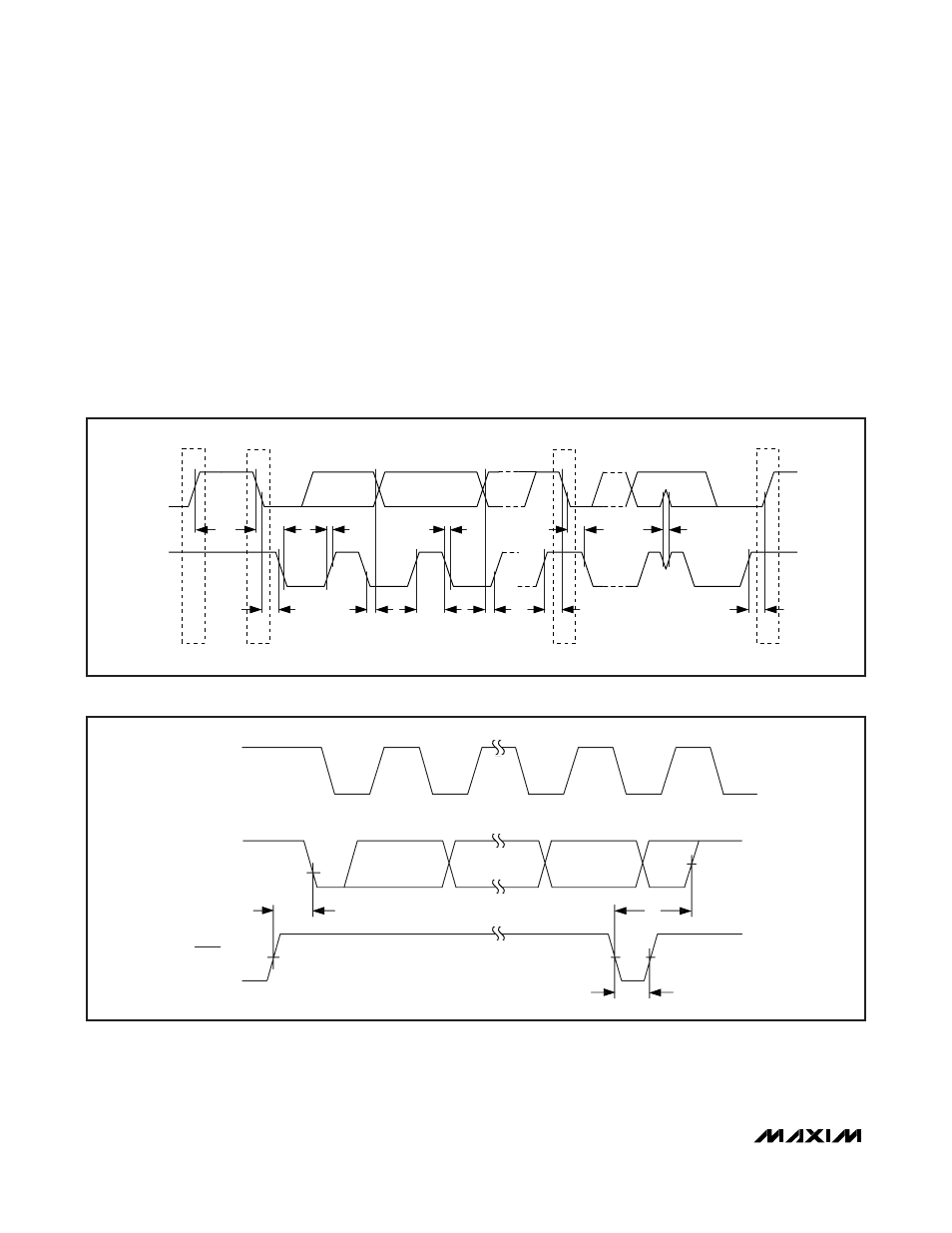
SDA
SCL
t
BUF
t
SU;STO
t
SP
t
HD;STA
t
SU;STA
t
F
t
HIGH
t
HD;DAT
t
R
t
LOW
t
HD;STA
S
P
Sr
P
t
SU;DAT
Figure 1. 2-Wire Serial-Interface Timing Diagram
SCL
SDA
RESET
t
REC;STA
t
WL(rst)
t
rst
Figure 2. RST Timing Diagram