Table 4. switch control register channel selection – Rainbow Electronics MAX7358 User Manual
Page 13
MAX7356/MAX7357/MAX7358
1-to-8 I
2
C Bus Switches/Multiplexers with Bus
Lock-Up Detection, Isolation, and Notification
______________________________________________________________________________________
13
Only the switch control register can be accessed through
an I
2
C write or read command. All data bytes are for
the switch control register. The last data byte in an I
2
C
write command is retained by the switch control register.
Register Access Protocol
(MAX7357/MAX7358)
Only the MAX7357 or MAX7358 I
2
C device address is
required to gain access to its registers. A typical I
2
C
command to communicate with the MAX7357 or
MAX7358 starts with its device address and is followed
directly by data bytes. Internal register addresses are
not used in an I
2
C write or read command.
For enhanced mode, all registers are accessed in
sequence starting with the switch control register and
follows the order defined by internal register addresses
as shown in Table 2. Internal register addresses are
0x00, 0x01, 0x02, 0x03, 0x04, 0x05, and 0x06 for
switch control, configuration, flush-out sequence, lock-
up indication, first and second bytes of the traffic prior
to lock-up, and preconnection fault registers, respec-
tively. When writing data to the register(s), addressing
starts with address 0x00 and goes one higher in each
subsequent byte and comes back to 0x00 again after
0x02 since the next four higher addressed registers are
read only. Read access also starts with the internal reg-
ister address 0x00 and goes one higher in each subse-
quent byte and comes back to 0x00 again after 0x06.
For basic mode, only the switch control register can be
accessed through an I
2
C write or read command. All
data bytes are for the switch control register. The last
data byte in an I
2
C write command is retained by the
switch control register. Incomplete bytes are ignored.
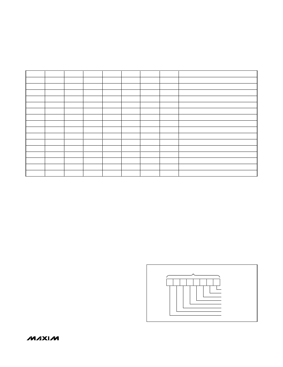
Switch Control Register
The switch control register (Figure 8) selects which
channels will be connected to the main I
2
C bus. This
register can be written and read through the main I
2
C
bus. The POR value for the switch control register is
0x00—all switches disconnected.
A SC_/SD_ downstream pair, or channel, is selected by
the contents of the switch control register. All bits of the
control byte are used to determine which channel is to
B6
B0
B7
B5
B4
B3
B2
B1
CHANNEL SELECTION BITS (READ/WRITE)
CHANNEL 0
CHANNEL 1
CHANNEL 2
CHANNEL 3
CHANNEL 4
CHANNEL 5
CHANNEL 6
CHANNEL 7
Figure 8. Switch Control Register
B7
B6
B5
B4
B3
B2
B1
B0
COMMAND
X
X
X
X
X
X
X
0
Channel 0 disabled
X
X
X
X
X
X
X
1
Channel 0 enabled
X
X
X
X
X
X
0
X
Channel 1 disabled
X
X
X
X
X
X
1
X
Channel 1 enabled
X
X
X
X
X
0
X
X
Channel 2 disabled
X
X
X
X
X
1
X
X
Channel 2 enabled
X
X
X
X
0
X
X
X
Channel 3 disabled
X
X
X
X
1
X
X
X
Channel 3 enabled
X
X
X
0
X
X
X
X
Channel 4 disabled
X
X
X
1
X
X
X
X
Channel 4 enabled
X
X
0
X
X
X
X
X
Channel 5 disabled
X
X
1
X
X
X
X
X
Channel 5 enabled
X
0
X
X
X
X
X
X
Channel 6 disabled
X
1
X
X
X
X
X
X
Channel 6 enabled
0
X
X
X
X
X
X
X
Channel 7 disabled
1
X
X
X
X
X
X
X
Channel 7 enabled
Table 4. Switch Control Register Channel Selection
X = Don’t care.