Rainbow Electronics MAX7358 User Manual
Page 2
MAX7356/MAX7357/MAX7358
1-to-8 I
2
C Bus Switches/Multiplexers with Bus
Lock-Up Detection, Isolation, and Notification
2
_______________________________________________________________________________________
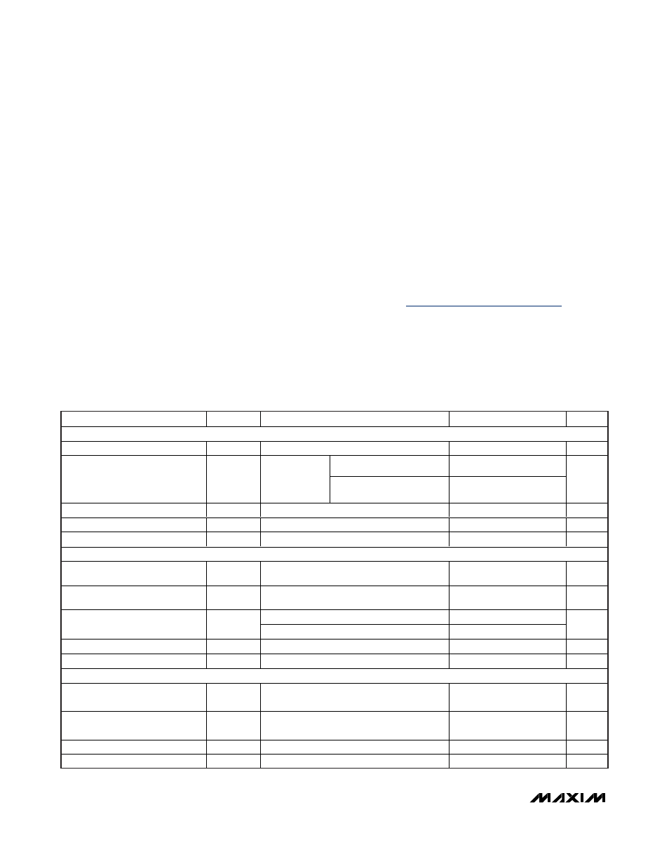
ABSOLUTE MAXIMUM RATINGS
ELECTRICAL CHARACTERISTICS (3.3V SUPPLY)
(V
DD
= +2.3V to +3.6V, T
A
= -40°C to +85°C, unless otherwise noted. Typical values are at V
DD
= +3.3V, T
A
= +25°C.) (Notes 2–5)
Stresses beyond those listed under “Absolute Maximum Ratings” may cause permanent damage to the device. These are stress ratings only, and functional
operation of the device at these or any other conditions beyond those indicated in the operational sections of the specifications is not implied. Exposure to
absolute maximum rating conditions for extended periods may affect device reliability.
Note 1: Package thermal resistances were obtained using the method described in JEDEC specification JESD51-7, using a 4-layer
board. For detailed information on package thermal considerations, refer to
www.maxim-ic.com/thermal-tutorial
.
(Voltages referenced to GND.)
V
DD
.................................................................. -0.3V to +6.0V
All Other Pins.....................................................-0.3V to +6.0V
Input Currents
V
DD
...............................................................................100mA
GND ..............................................................................100mA
All Input Pins.....................................................................±20mA
Output Current ....................................................................25mA
Continuous Power Dissipation (T
A
= +70°C)
24-Pin TSSOP (derate 13.9mW/°C above +70°C) .....1111mW
24-Pin TQFN (derate 27.8mW/°C above +70°C) .......2222mW
Junction-to-Case Thermal Resistance (
θ
JC
) (Note 1)
24-Pin TSSOP...............................................................13°C/W
24-Pin TQFN................................................................3.0°C/W
Junction-to-Ambient Thermal Resistance (
θ
JA
) (Note 1)
24-Pin TSSOP............................................................72.0°C/W
24-Pin TQFN..............................................................36.0°C/W
Operating Temperature Range ......................... -40°C to +85°C
Junction Temperature .................................................... +150°C
Storage Temperature Range ........................... -65°C to +150°C
Lead Temperature (soldering, 10s) ................................+300°C
PARAMETER
SYMBOL
CONDITIONS
MIN
TYP
MAX
UNITS
POWER SUPPLY
Supply Voltage
V
DD
2.3
3.6
V
Basic mode
30
50
Supply Current
I
DD
V
DD
= 3.6V;
no load, f
SCL
=
400kHz
Enhanced mode
(MAX7357/MAX7358 only)
45
70
µA
Standby Current
I
STB
No load, V
I
= V
DD
or GND, V
DD
= 3.6V
0.1
1
µA
Power-On Reset Voltage
V
POR
V
DD
rising
0.9
1.4
2.1
V
Power-On Reset Hysteresis
V
HYST
0.4
V
INPUT SCL, INPUT/OUTPUT SDA
Low-Level Input Voltage
V
IL
0.3 x
V
DD
V
High-Level Input Voltage
V
IH
0.7 x
V
DD
V
V
OL
= 0.4V
3
Low-Level Output Current
I
OL
V
OL
= 0.6V
6
mA
Input Leakage Current
I
LH
, I
LI
V
SCL
and V
SDA
= V
DD
or GND
-1
+1
µA
Input Capacitance
C
I
V
I
= GND
15
pF
SELECT INPUTS A0 to A2,
RST
Low-Level Input Voltage
V
IL
0.3 x
V
DD
V
High-Level Input Voltage
V
IH
0.7 x
V
DD
V
Input Leakage Current
I
LI
A0 to A2, and
RST at V
DD
or GND
-1
+1
µA
Input Capacitance
C
I
V
I
= GND
2
pF