Applications information, Chip information, Voltage level translation – Rainbow Electronics MAX7358 User Manual
Page 20
MAX7356/MAX7357/MAX7358
1-to-8 I
2
C Bus Switches/Multiplexers with Bus
Lock-Up Detection, Isolation, and Notification
20
______________________________________________________________________________________
ADDRESS OF MUX/SWT PART
S
START
0
A
D7
D6
D5
D4
D3
D2
D1
D0
A
P
R/W
ACKNOWLEDGE FROM THE
MAX7357 OR MAX7358
ACKNOWLEDGE FROM THE
MAX7357 OR MAX7358
STOP
DATA BYTE TO THE SWITCH
CONTROL REGISTER
D7
D6
D5
D4
D3
D2
D1
D0
A
ACKNOWLEDGE FROM THE
MAX7357 OR MAX7358
DATA BYTE TO THE SWITCH
CONTROL REGISTER
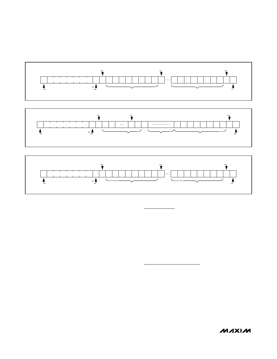
Figure 17. Reading the MAX7356
ADDRESS OF MUX/SWT PART
S
START
1
A
D7
D6
D1
D0
A
P
R/W
ACKNOWLEDGE FROM THE
MAX7357 OR MAX7358
ACKNOWLEDGE
FROM A HOST
STOP
DATA BYTE FROM THE SWITCH
CONTROL REGISTER
DATA BYTE FROM
REGISTERS
0X01 TO 0X06
D7
D6
D5
D4
D3
D2
D1
D0
A
ACKNOWLEDGE FROM A
HOST
DATA BYTE FROM THE
STUCK HIGH FAULT REGISTER
Figure 18. Reading the MAX7357 or MAX7358 in Enhanced Mode
ADDRESS OF MUX/SWT PART
S
START
1
A
D7
D6
D5
D4
D3
D2
D1
D0
A
P
R/W
ACKNOWLEDGE FROM THE
MAX7357 OR MAX7358
ACKNOWLEDGE FROM A
HOST
STOP
DATA BYTE FROM THE SWITCH
CONTROL REGISTER
D7
D6
D5
D4
D3
D2
D1
D0
A
ACKNOWLEDGE FROM A
HOST
DATA BYTE FROM THE SWITCH
CONTROL REGISTER
Figure 19. Reading the MAX7357 or MAX7358 in Basic Mode
Reading from the MAX7357/MAX7358
in Basic Mode
A read from the MAX7357 or MAX7358 in basic mode
starts with the master transmitting the slave address
with the R/W bit set high. The device acknowledges the
slave address. The master can read 1 byte from the
switch control register and then issue a STOP condition
(Figure 19). If the master reads more than one byte, the
master upon reception acknowledges each byte. All
bytes return the contents of the switch control register.
Applications Information
Voltage Level Translation
The pass gates of the MAX7356/MAX7357/MAX7358
are designed so V
DD
can be used to limit the voltage
levels transferred from one bus to another. The power-
supply voltage of the part should be selected to be no
larger than one VGS
ON
(0.7V, typ) above the lowest
bus voltage in the system. This ensures that the analog
switches do not allow current to flow from higher volt-
age buses to lower voltage buses.
Chip Information
PROCESS: CMOS