Electrical characteristics (5v supply) (continued) – Rainbow Electronics MAX7358 User Manual
Page 4
MAX7356/MAX7357/MAX7358
1-to-8 I
2
C Bus Switches/Multiplexers with Bus
Lock-Up Detection, Isolation, and Notification
4
_______________________________________________________________________________________
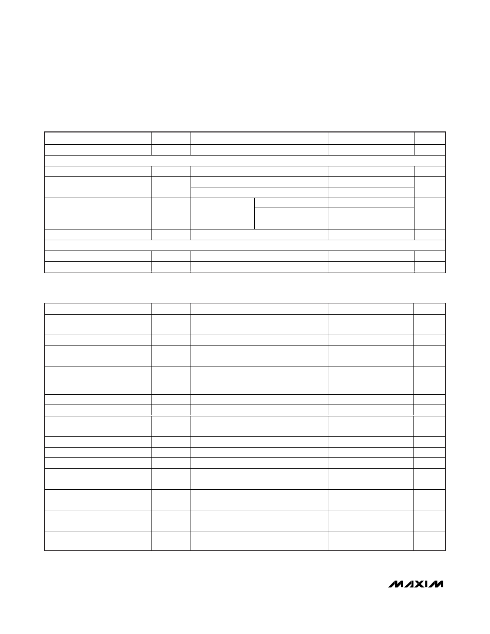
TIMING CHARACTERISTICS (STANDARD-MODE) (Figures 1, 2, 3)
(V
DD
= 2.3V to 5.5V, T
A
= -40°C to +85°C, unless otherwise noted.) (Notes 2, 6)
PARAMETER
SYMBOL
CONDITIONS
MIN
TYP
MAX
UNITS
Propagation Delay from SDA to
SD_ or SCL to SC_
t
PD
(Note 7)
0.3
ns
SCL Clock Frequency
f
SCL
0
100
kHz
Bus Free Time Between a STOP
and START Condition
t
BUF
4.7
µs
Hold Time (Repeated) START
Condition After this Period, the
First Clock Pulse is Generated
t
HD;STA
4.0
µs
LOW Period of the SCL Clock
t
LOW
4.7
µs
HIGH Period of the SCL Clock
t
HIGH
4.0
µs
Setup Time for a Repeated
START Condition
t
SU;STA
4.7
µs
Setup Time for a STOP Condition
t
SU;STO
4.0
µs
Data Hold Time
t
HD;DAT
(Note 8)
0
3.45
µs
Data Setup Time
t
SU;DAT
250
ns
Rise Time of Both SDA and SCL
Signals
t
R
1000
ns
Fall Time of Both SDA and SCL
Signals
t
F
300
ns
Capacitive Load for Each Bus
Line
C
b
400
pF
Pulse Width of Spikes that Must
be Suppressed by the Input Filter
t
SP
50
ns
ELECTRICAL CHARACTERISTICS (5V SUPPLY) (continued)
(V
DD
= +4.5V to +5.5V, T
A
= -40°C to +85°C, unless otherwise noted. Typical values are at V
DD
= +5V, T
A
= +25°C.) (Notes 2–5)
PARAMETER
SYMBOL
CONDITIONS
MIN
TYP
MAX
UNITS
Input Capacitance
C
I
V
I
= GND
2
pF
PASS GATE
Switch Resistance
R
ON
V
DD
= 4.5V to 5.5V, V
O
= 0.4V, I
O
= 15mA
4
9
24
Ω
V
SWin
= V
DD
= 5.0V, I
SWout
= -100µA
3.6
Switch Output Voltage
V
SW
V
S Wi n
= V
D D
= 4.5V to 5.5V , I
S Wo ut
= - 100µA
2.6
4.5
V
MAX7356
-1
+1
Leakage Current
I
L
V
I
= V
DD
or GND
Enhanced mode
(MAX7357/MAX7358)
-2
+2
µA
Input/Output Capacitance
C
IO
V
I
= GND
3
pF
OUTPUT
RST/INT
Low-Level Output Current
I
OL
V
OL
= 0.4V (MAX7357/MAX7358)
3
mA
Leakage Current
I
LH
, I
LI
V
RST/INT
= V
DD
or GND
-1
+1
µA