Chip information, Package information – Rainbow Electronics MAX17000 User Manual
Page 31
MAX17000
Complete DDR2 and DDR3 Memory
Power-Management Solution
Maxim cannot assume responsibility for use of any circuitry other than circuitry entirely embodied in a Maxim product. No circuit patent licenses are
implied. Maxim reserves the right to change the circuitry and specifications without notice at any time.
Maxim Integrated Products, 120 San Gabriel Drive, Sunnyvale, CA 94086 408-737-7600 ____________________ 31
© 2008 Maxim Integrated Products
is a registered trademark of Maxim Integrated Products, Inc.
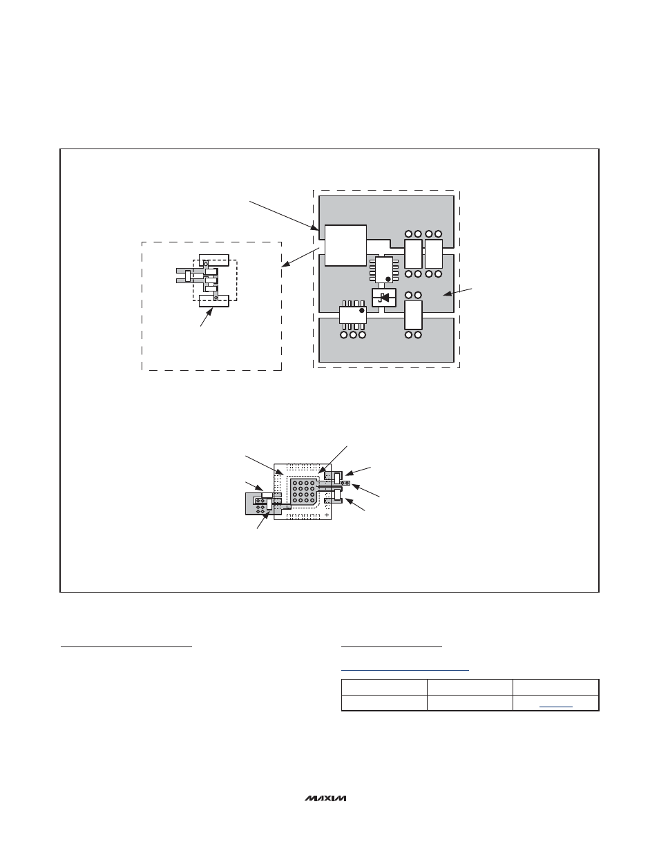
KELVIN SENSE VIAS
UNDER THE INDUCTOR
(SEE EVALUATION KIT)
VIA TO POWER GROUND
CONNECT AGND AND PGND1 TO
THE CONTROLLER AT THE
EXPOSED PAD
CONNECT THE
EXPOSED PAD TO
ANALOG GROUND
X-RAY VIEW.
IC MOUNTED
ON BOTTOM
SIDE OF PCB.
POWER STAGE LAYOUT (TOP SIDE OF PCB)
IC LAYOUT
V
DD
BYPASS
CAPACITOR
V
CC
BYPASS
CAPACITOR
VTTI BYPASS
CAPACITOR
VTT BYPASS
CAPACITOR
INDUCTOR
L1
OUTPUT
SMPS
C
OUT
INPUT
POWER
GROUND
C
EQ
CSL
CSH
R2
R1
R
NTC
KELVIN-SENSE VIAS TO
INDUCTOR PAD
INDUCTOR DCR SENSING
C
OUT
C
IN1
Figure 9. PCB Layout Example
Chip Information
TRANSISTOR COUNT: 7856
PROCESS: BiCMOS
Package Information
For the latest package outline information, go to
www.maxim-ic.com/packages
.
PACKAGE TYPE
PACKAGE CODE
DOCUMENT NO.
24 TQFN
T2444-1