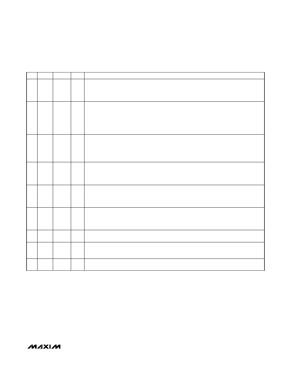
Table 3. operating mode truth table – Rainbow Electronics MAX17000 User Manual
Page 15
MAX17000
Complete DDR2 and DDR3 Memory
Power-Management Solution
______________________________________________________________________________________
15
SHDN STDBY SKIP
OPERATION
1
L
→ H
L
→ H
X
SMPS output ramps up in skip mode with a 1.4ms (typ) ramp time. PGOOD1 is held low until the
SMPS output is in regulation.
VTT and VTTR ramp up to the final voltage based on V
CSL
/2 or V
REFIN
. PGOOD2 is held low until
VTT is in regulation.
2
L
→ H
L
X
SMPS output ramps up in skip mode with a 1.4ms ramp time. PGOOD1 is held low until the SMPS
output is in regulation.
O nce C S L or FB i s i n r eg ul ati on, the P W M b l ock tur ns off and enter s stand b y m od e.
VTT remains off throughout since
STDBY is low. PGOOD2 stays low throughout. The VTT discharge
FET is enabled if OVP is high, but disabled if OVP is low.
VTTR ramps up to the final voltage based on V
CSL
/2 or V
REFIN
.
3
H
L
→ H
X
Ultra-skip and standby modes are exited and the full current capability of the MAX17000 is
available.
VTT ramps up after the internal SMPS block is ready. VTT ramps to the final voltage based on
V
CSL
/2 or V
REFIN
.
PGOOD2 goes high when VTT is in regulation.
4
H
H
H
SMPS output is in forced-PWM mode.
VTT and VTTR are enabled.
PGOOD1 is high when the SMPS output is in regulation.
PGOOD2 is high when VTT is in regulation.
5
H
H
L
SMPS output is in normal skip mode.
VTT and VTTR are enabled.
PGOOD1 is high when the SMPS output is in regulation.
PGOOD2 is high when VTT is in regulation.
6
H
L
X
SMPS output is in ultra-skip mode.
VTT is off and is high impedance.
PGOOD2 is forced low.
VTTR is active and regulates to V
CSL
/2 or V
REFIN
.
7
H
→ L
H
X
U l tr a- ski p or ski p m od e i s exi ted as the M AX 17000 r am p s the outp ut d ow n to zer o.
V TTR tr acks V
C S L
/2 or V
R E F IN
d ur i ng shutd ow n. After the S M P S outp ut r eaches 25m V , D L g oes l ow .
8
H
→ L
L
X
Ultra-skip or skip mode is exited as the MAX17000 ramps the output down to zero.
VTTR tracks V
CSL
/2 or V
REFIN
during shutdown. After the SMPS output reaches 25mV, DL goes
low. VTT is not enabled throughout soft-shutdown.
9
L
X
X
DL low. Internal16
Ω discharge MOSFETs on CSL and VTT enabled if OVP is high, but disabled if
OVP is low.
Table 3. Operating Mode Truth Table