Rainbow Electronics MAX17000 User Manual
Page 28
MAX17000
Complete DDR2 and DDR3 Memory
Power-Management Solution
28
______________________________________________________________________________________
where I
VALLEY(MAX)
is the maximum valley current
allowed by the current-limit circuit, including threshold
tolerance and on-resistance variation. The MOSFETs
must have a good size heatsink to handle the overload
power dissipation.
Choose a Schottky diode (DL) with a forward voltage
low enough to prevent the low-side MOSFET body
diode from turning on during the dead time. Select a
diode that can handle the load current during the dead
times. This diode is optional and can be removed if effi-
ciency is not critical.
Setting the PWM Output Voltage
Preset Output Voltages
The MAX17000’s Dual Mode™ operation allows the
selection of common voltages without requiring external
components. Connect FB to AGND for a fixed 1.5V out-
put, to V
CC
for a fixed 1.8V output, or connect FB
directly to OUT for a fixed 1.0V output.
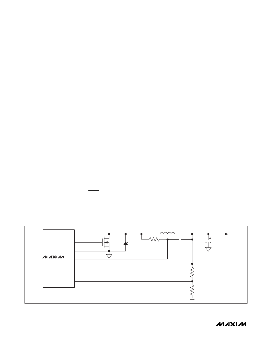
Adjustable Output Voltage
The output voltage can be adjusted from 1.0V to 2.7V
using a resistive voltage-divider (Figure 8). The
MAX17000 regulates FB to a fixed reference voltage
(1.0V). The adjusted output voltage is:
where V
FB
is 1.0V.
VTTI Input Capacitor
Stability Considerations
The value of the VTTI bypass capacitor is chosen to
limit the amount of ripple/noise at VTTI, and the amount
of voltage dip during a load transient. Typically, VTTI is
connected to the output of the buck regulator, which
already has a large bulk capacitor. Nevertheless, a
ceramic capacitor of equivalent value to the VTT output
capacitor must be used and must be added and
placed as close as possible to the VTTI pin. This value
must be increased with larger load current, or if the
trace from the VTTI pin to the power source is long and
has significant impedance.
Setting VTT Output Voltage
The VTT output stage is powered from the VTTI input.
The output voltage is set by the REFIN input. REFIN sets
the feedback regulation voltage (VTTR = VTTS =
V
REFIN
) of the MAX17000. Connect a 0.1V to 2.0V volt-
age input to set the adjustable output for VTT, VTTS, and
VTTR. If REFIN is tied to V
CC
, the internal CSL/2 divider
is used to set VTT voltage; hence, VTT tracks the V
CSL
voltage and is set to V
CSL
/2. This feature makes the
MAX17000 ideal for memory applications in which the
termination supply must track the supply voltage.
VTT Output Capacitor Selection
A minimum value of 9μF is needed to stabilize a 300mA
VTT output. This value of capacitance limits the regula-
tor’s unity-gain bandwidth frequency to approximately
1.2MHz (typ) to allow adequate phase margin for stabil-
ity. To keep the capacitor acting as a capacitor within
the regulator’s bandwidth, it is important that ceramic
capacitors with low ESR and ESL be used.
V
V
R
R
OUT
FB
FBA
FBB
=
× +
⎛
⎝⎜
⎞
⎠⎟
1
FB
V
OUT
PGND1
DL
LX
CSL
C
OUT
L1
N
L
D1
R
FBA
R
FBB
CSH
MAX17000
Figure 8. Setting VOUT with a Resistive Voltage-Divider
Dual Mode is a trademark of Maxim Integrated Products, Inc.