Pin description – Rainbow Electronics MAX17000 User Manual
Page 12
MAX17000
Complete DDR2 and DDR3 Memory
Power-Management Solution
12
______________________________________________________________________________________
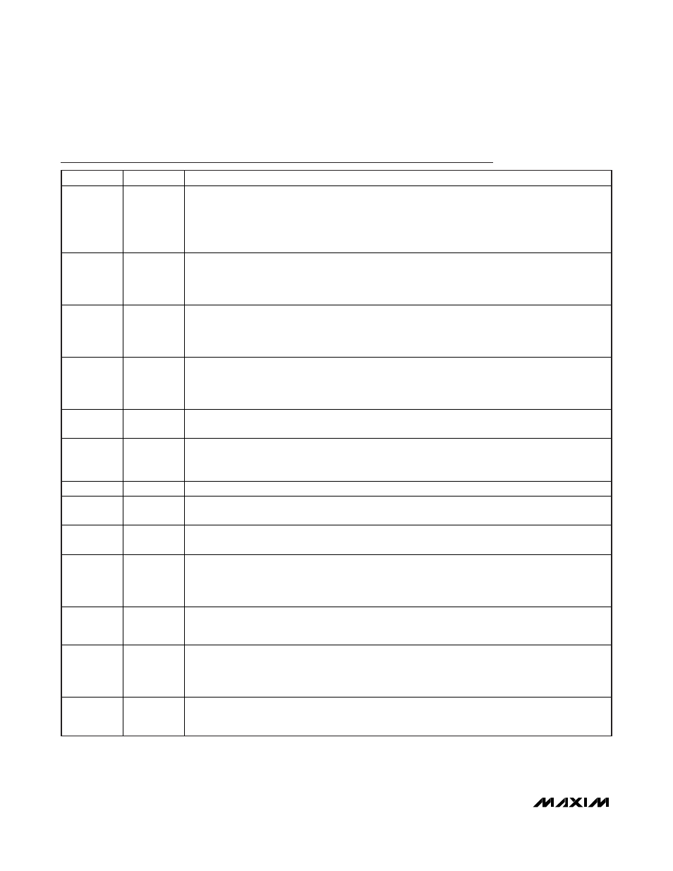
Pin Description
PIN
NAME
FUNCTION
1
OVP
OVP Mode Control. This input selectively enables/disables the SMPS OV protection feature and
output discharge mode. When enabled, the SMPS OV protection feature is enabled. Connect OVP to
the following voltage levels for the desired function:
High (> 2.4V) = Enable SMPS OV protection, and SMPS and VTT discharge FETs.
Low (GND) = Disable SMPS OV protection, and SMPS and VTT discharge FETs.
2
PGOOD1
Open-Drain Power-Good Output. PGOOD1 is low when the SMPS output voltage is more than 15%
(typ) beyond the normal regulation point, during soft-start, and in shutdown.
After the soft-start circuit has terminated, PGOOD1 becomes high impedance if the SMPS output is in
regulation.
3
PGOOD2
Open-Drain Power-Good Output. PGOOD2 is low when the VTT output voltage is more than 10% (typ)
beyond the normal regulation point, in shutdown, and in standby.
After the SMPS soft-start circuit has terminated, PGOOD2 becomes high impedance if the VTT output
is in regulation.
4
STDBY
Standby Control Input. When
SHDN is high and STDBY is low, the MAX17000 enters a low-quiescent
current mode, putting the SMPS in ultra-skip operation and turning off the VTT output (high-Z). This
mode helps save converter power loss in computer standby operation.
When
STDBY is high, normal SMPS operation resumes and the VTT output is enabled.
5
VTTS
Sense Pin for Termination Supply Output. Normally connected to the VTT pin to allow accurate
regulation to V
CSL
/2 or the REFIN voltage.
6
VTTR
Termination Reference Buffer Output. VTTR tracks V
CSL
/2 when REFIN is connected to V
CC
. VTTR
tracks V
REFIN
when a voltage between 0.5V to 1.5V is set at REFIN. Decouple VTTR to AGND with a
0.33μF ceramic capacitor.
7
PGND2
Power Ground for VTT. Connect PGND2 externally to the underside of the exposed pad.
8
VTT
Termination Power-Supply Output. Connect VTT to VTTS to regulate the VTT voltage to the VTTS
regulation setting.
9
VTTI
Termination Power-Supply Input. VTTI is the input power supply to the VTT linear regulator. Normally
connected to the output of the SMPS regulator for DDR applications.
10
REFIN
External Reference Input. REFIN sets the feedback regulation voltage (VTTR = VTTS = V
REFIN
) of the
MAX17000.
Connect REFIN to V
CC
to use the internal V
CSL
/2 divider.
Connect a 0.5V to 1.5V voltage input to set the adjustable output for VTT, VTTS, and VTTR.
11
FB
Feedback Input for SMPS Output. Connect to V
CC
for a fixed +1.8V output or to AGND for a fixed
+1.5V output. For an adjustable output (1.0V to 2.7V), connect FB to a resistive divider from the output
voltage. FB regulates to +1.0V.
12
CSL
Negative Input of the PWM Output Current-Sense and Supply Input for VTTR. Connect CSL to the
negative side of the output current-sensing resistor or the filtering capacitor if the DC resistance of the
output inductor is utilized for current sensing.
C S L i s al so the p ath for the i nter nal 16
_ d i schar g e M OS FE T w hen V
C C
U V LO occur s w i th OV P enab l ed .
13
CSH
Positive Input of the PWM Output Current Sense. Connect CSH to the positive side of the output
current-sensing resistor or the filtering capacitor if the DC resistance of the output inductor is utilized
for current sensing.