Rainbow Electronics MAX17000 User Manual
Page 25
MAX17000
Complete DDR2 and DDR3 Memory
Power-Management Solution
______________________________________________________________________________________
25
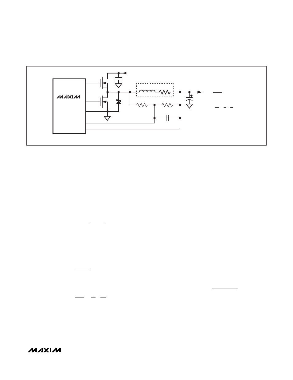
For the best current-sense accuracy and overcurrent
protection, use a 1% tolerance current-sense resistor
between the inductor and output as shown in Figure 7a.
This configuration constantly monitors the inductor cur-
rent, allowing accurate current-limit protection.
However, the parasitic inductance of the current-sense
resistor can cause current-limit inaccuracies, especially
when using low-value inductors and current-sense
resistors. This parasitic inductance (L
ESL
) can be can-
celled by adding an RC circuit across the sense resis-
tor with an equivalent time constant:
Alternatively, low-cost applications that do not require
highly accurate current-limit protection could reduce
the overall power dissipation by connecting a series RC
circuit across the inductor (Figure 7b) with an equiva-
lent time constant:
and:
where R
CS
is the required current-sense resistance,
and R
DCR
is the inductor’s series DC resistance. Use
the worst-case inductance and R
DCR
values provided
by the inductor manufacturer, adding some margin for
the inductance drop over temperature and load.
MOSFET Gate Drivers (DH, DL)
The DH and DL drivers are optimized for driving moder-
ate-sized high-side, and larger low-side power MOSFETs.
This is consistent with the low duty factor seen in note-
book applications, where a large V
IN
- V
OUT
differential
exists. The high-side gate driver (DH) sources and sinks
1.2A, and the low-side gate driver (DL) sources 1.0A and
sinks 2.4A. This ensures robust gate drive for high-cur-
rent applications. The DH floating high-side MOSFET dri-
ver is powered by an internal boost switch charge pump
at BST, while the DL synchronous-rectifier driver is pow-
ered directly by the 5V bias supply (V
DD
).
PWM Output Capacitor Selection
The output filter capacitor must have low enough effec-
tive series resistance (ESR) to meet output ripple and
load-transient requirements, yet have high enough ESR
to satisfy stability requirements.
In core and chipset converters and other applications
where the output is subject to large-load transients, the
output capacitor’s size typically depends on how much
ESR is needed to prevent the output from dipping too
low under a load transient. Ignoring the sag due to finite
capacitance:
In low-power applications, the output capacitor’s size
often depends on how much ESR is needed to maintain
an acceptable level of output ripple voltage. The output
ripple voltage of a step-down controller equals the total
inductor ripple current multiplied by the output capaci-
tor’s ESR.
R
R
V
I
ESR
PCB
STEP
LOAD MAX
+
(
)
≤
Δ
(
)
R
L
C
R
R
DCR
EQ
=
×
+
⎡
⎣⎢
⎤
⎦⎥
1
1
1
2
R
R
R
R
R
CS
DCR
=
+
×
2
1
2
C
R
L
R
EQ
EQ
ESL
SENSE
×
=
MAX17000
C
OUT
INPUT (V
IN
)
C
IN
B) LOSSLESS INDUCTOR SENSING
FOR THERMAL COMPENSATION:
R2 SHOULD CONSIST OF AN NTC RESISTOR IN
SERIES WITH A STANDARD THIN-FILM RESISTOR.
CSL
CSH
PGND1
DL
DH
LX
C
EQ
R
1
R
2
N
H
N
L
D
L
L
INDUCTOR
R
DCR
R
CS
=
R2
R
DCR
R1 + R2
R
DCR
=
L
[
1 + 1
]
C
EQ
R1 R2
Figure 7b. Current-Sense Configurations (Sheet 2 of 2)