Rainbow Electronics MAX17000 User Manual
Page 24
MAX17000
Complete DDR2 and DDR3 Memory
Power-Management Solution
24
______________________________________________________________________________________
stresses and thus drives the selection of input
capacitors, MOSFETs, and other critical heat-con-
tributing components. Most notebook loads gener-
ally exhibit I
LOAD
= I
LOAD(MAX)
x 80%.
•
Switching Frequency: This choice determines the
basic trade-off between size and efficiency. The
optimal frequency is largely a function of maximum
input voltage, due to MOSFET switching losses that
are proportional to frequency and V
IN
2
. The opti-
mum frequency is also a moving target, due to
rapid improvements in MOSFET technology that are
making higher frequencies more practical.
•
Inductor Operating Point: This choice provides
trade-offs between size vs. efficiency and transient
response vs. output noise. Low inductor values pro-
vide better transient response and smaller physical
size, but also result in lower efficiency and higher
output noise due to increased ripple current. The
minimum practical inductor value is one that causes
the circuit to operate at the edge of critical conduc-
tion (where the inductor current just touches zero
with every cycle at maximum load). Inductor values
lower than this grant no further size-reduction bene-
fit. The optimum operating point is usually found
between 20% and 50% ripple current.
Inductor Selection
The switching frequency and operating point (% ripple
current or LIR) determine the inductor value as follows:
Find a low-loss inductor having the lowest possible DC
resistance that fits in the allotted dimensions. Ferrite
cores are often the best choice, although powdered
iron is inexpensive and can work well at 200kHz. The
core must be large enough not to saturate at the peak
inductor current (I
PEAK
):
Setting the Valley Current Limit
The minimum current-limit threshold must be high
enough to support the maximum load current when the
current limit is at the minimum tolerance value. The val-
ley of the inductor current occurs at I
LOAD(MAX)
minus
half the ripple current; therefore:
where I
LIMIT(LOW)
equals the minimum current-limit
threshold voltage divided by the output sense element
(inductor DCR or sense resistor).
The valley current limit is fixed at 17mV (min) across the
CSH to CSL differential input.
Special attention must be made to the tolerance and
thermal variation of the on-resistance in the case of DCR
sensing. Use the worst-case maximum value for R
DCR
from the inductor data sheet, and add some margin for
the rise in R
DCR
with temperature. A good general rule
is to allow 0.5% additional resistance for each °C of
temperature rise, which must be included in the design
margin unless the design includes an NTC thermistor in
the DCR network to thermally compensate the current-
limit threshold.
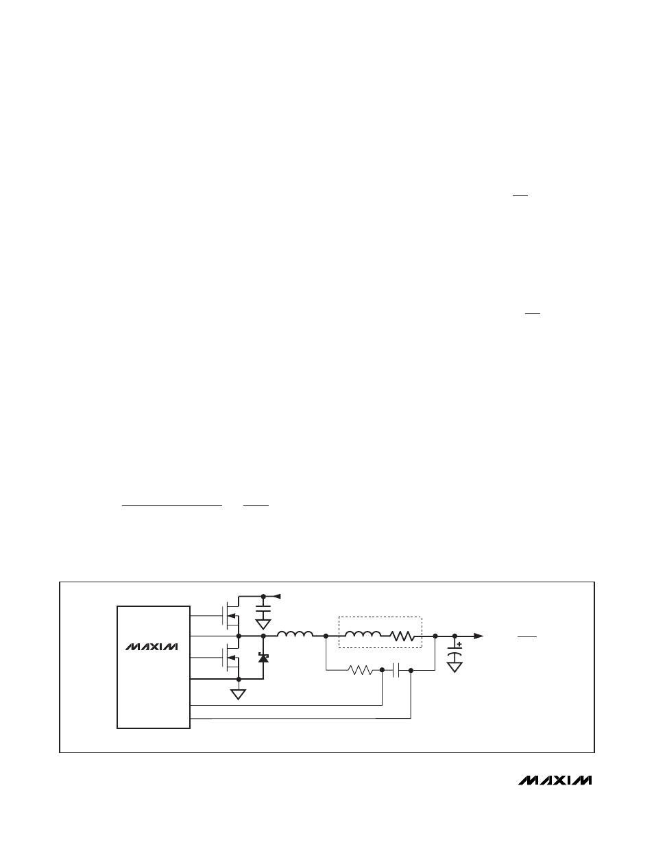
The current-sense method (Figure 7) and magnitude
determine the achievable current-limit accuracy and
power loss. The sense resistor can be determined by:
R
SENSE
= V
LIMIT
/I
LIMIT
I
I
LIR
LIMIT LOW
LOAD MAX
(
)
(
)
>
× −
⎛
⎝⎜
⎞
⎠⎟
1
2
I
I
LIR
PEAK
LOAD MAX
=
× +
⎛
⎝⎜
⎞
⎠⎟
(
)
1
2
L
V
V
f
I
LIR
V
V
IN
OUT
SW
LOAD MAX
OUT
IN
=
−
Ч
Ч
⎛
⎝
⎜
⎞
⎠
⎟ Ч
⎛
(
)
⎝⎝⎜
⎞
⎠⎟
SENSE RESISTOR
L
MAX17000
C
OUT
INPUT (V
IN
)
C
IN
CSL
CSH
PGND1
DL
DH
LX
C
EQ
R
EQ
N
H
N
L
D
L
L
ESL
R
SENSE
C
EQ
R
EQ
=
L
ESL
R
SENSE
A) OUTPUT SERIES RESISTOR SENSING
Figure 7a. Current-Sense Configurations (Sheet 1 of 2)