Detailed description – Rainbow Electronics MAX17000 User Manual
Page 16
MAX17000
Complete DDR2 and DDR3 Memory
Power-Management Solution
16
______________________________________________________________________________________
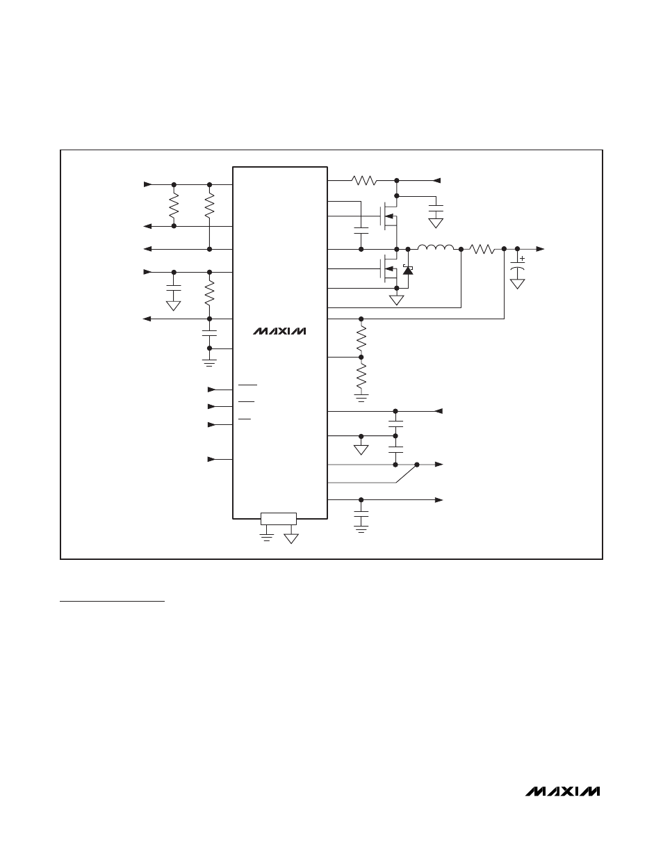
Detailed Description
The MAX17000 complete DDR solution comprises a
step-down controller, a source-sink LDO regulator, and a
reference buffer. Maxim’s proprietary Quick-PWM pulse-
width modulator in the MAX17000 is specifically
designed for handling fast load steps while maintaining a
relatively constant operating frequency and inductor
operating point over a wide range of input voltages. The
Quick-PWM architecture circumvents the poor load-tran-
sient timing problems of fixed-frequency current-mode
PWMs, while also avoiding the problems caused by
widely varying switching frequencies in conventional con-
stant-on-time and constant-off-time PWM schemes.
Figure 1 is the MAX17000 standard application circuit
and Figure 2 is the MAX17000 functional diagram.
The MAX17000 includes a ±2A source-sink LDO regu-
lator for the memory termination rail. The source-sink
regulator features a dead band that either sources or
sinks, ideal for the fast-changing short-period loads
presenting in memory termination applications. This
feature also reduces the VTT output capacitance
requirement down to 1μF, though load-transient
response can still require higher capacitance values
between 10μF and 20μF.
The reference buffer sources and sinks ±3mA, generating
a reference rail for use in the memory controller and
memory devices.
DH
V
DD
V
CC
TON
ON/OFF
FB
BST
V
IN
7V TO 20V
VDDQ
+1.8V OR 1.5V
PGND1
DL
LX
CSL
C
IN
N
H
R
SENSE
N
L
R
FBA
R
FBB
C
VTTI
C
VTT
C
VTTR
0.33
μF
L1
D1
PGND2
VTTI
VTTR
VTTS
+5V
SLP_S3#
VTT
+1V TO + 2.5V
VTT = VDDQ/2
STDBY
SHDN
SKIP
REFIN
PGOOD2
+5V
PGOOD1
AGND
FB OPTIONS:
1. CONNECT FB TO 5V FOR FIXED +1.8V.
2. CONNECT FB TO GND FOR FIXED +1.5V.
3. USE FB RESISTOR-DIVIDER FOR ADJUSTABLE
OUTPUT VOLTAGES.
R
TON
CSH
5V V
CC
V
CC
OVP
1
12
16
18
4
24
7
6
20
14
15
17
13
23
22
21
19
10
9
2
3
EP
AGND
PGND
11
5
8
C
BST
0.1
μF
R3
100k
Ω
R2
100k
Ω
R1
10
Ω
C
VDD
1
μF
C
VCC
1
μF
AGND
AGND
PGND
AGND
PGND
PGND
PGND
PGND
C
OUT
MAX17000
VTTR = VDDQ/2
Figure 1. MAX17000 Standard Application Circuit