Boot rom containing bootstrap loader, Modify pc and start program execution immediately – Texas Instruments MSP430x11x1 User Manual
Page 9
MSP430x11x1
MIXED SIGNAL MICROCONTROLLER
SLAS241C – SEPTEMBER 1999 – REVISED JUNE 2000
9
POST OFFICE BOX 655303
•
DALLAS, TEXAS 75265
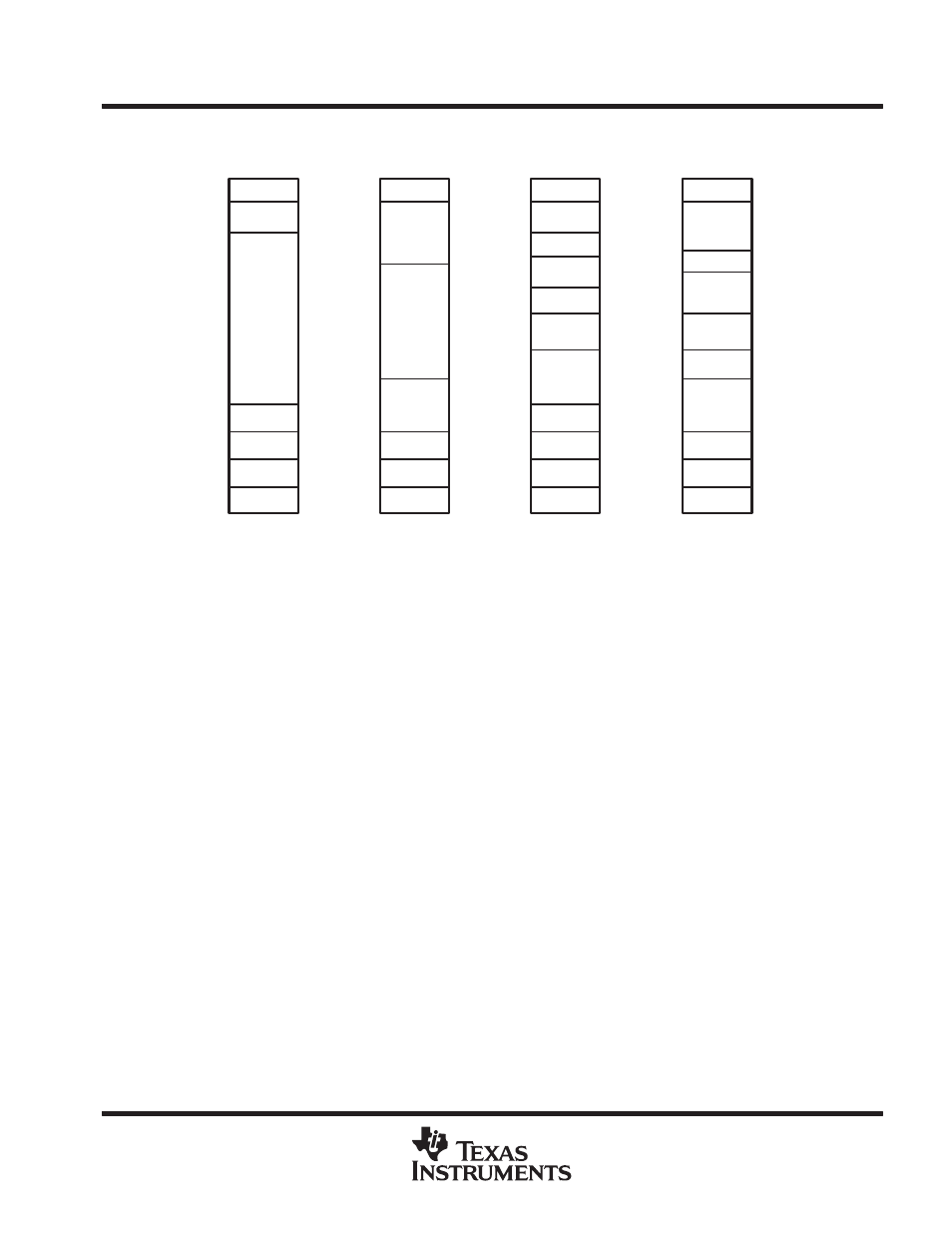
memory organization
Int. Vector
2 KB ROM
128B RAM
16b Per.
8b Per.
SFR
FFFFh
FFE0h
FFDFh
F800h
027Fh
0200h
01FFh
0100h
00FFh
0010h
000Fh
0000h
MSP430C1111
Int. Vector
4 KB
Flash
Segment0–7
256B RAM
16b Per.
8b Per.
SFR
FFFFh
FFE0h
FFDFh
02FFh
0200h
01FFh
0100h
00FFh
0010h
000Fh
0000h
MSP430F1121
Int. Vector
4 KB
ROM
256B RAM
16b Per.
8b Per.
SFR
FFFFh
FFE0h
FFDFh
F000h
02FFh
0200h
01FFh
0100h
00FFh
0010h
000Fh
0000h
MSP430C1121
F000h
Main
Memory
10FFh
2
×
128B
Flash
SegmentA,B
Information
Memory
1000h
1 KB
Boot ROM
0FFFh
0C00h
Int. Vector
1 KB Flash
Segment0,1
128B RAM
16b Per.
8b Per.
SFR
FFDFh
FC00h
027Fh
0200h
0100h
00FFh
0010h
000Fh
0000h
MSP430F1101
1 KB
Boot ROM
128B Flash
SegmentA
10FFh
1080h
01FFh
0C00h
0FFFh
FFFFh
FFE0h
boot ROM containing bootstrap loader
The intention of the bootstrap loader is to download data into the flash memory module. Various write, read, and
erase operations are needed for a proper download environment. The bootstrap loader is only available on F
devices.
functions of the bootstrap loader:
Definition of read:
apply and transmit data of peripheral registers or memory to pin P1.1 (BSLTX)
write:
read data from pin P2.2 (BSLRX) and write them into flash memory
unprotected functions
Mass erase, erase of the main memory (Segment0 to Segment7)
Access to the MSP430 via the bootstrap loader is protected. It must be enabled before any protected function
can be performed. The 256 bits in 0FFE0h to 0FFFFh provide the access key.
protected functions
All protected functions can be executed only if the access is enabled.
D
Write/program byte into flash memory; Parameters passed are start address and number of bytes (the
segment-write feature of the flash memory is not supported and not useful with the UART protocol).
D
Segment erase of Segment0 to Segment7 in the main memory and segment erase of SegmentA and
SegmentB in the information memory.
D
Read all data in main memory and information memory.
D
Read and write to all byte peripheral modules and RAM.
D
Modify PC and start program execution immediately.
NOTE:
Unauthorized readout of code and data is prevented by the user’s definition of the data in the
interrupt memory locations.