Texas Instruments MSP430x11x1 User Manual
Page 30
MSP430x11x1
MIXED SIGNAL MICROCONTROLLER
SLAS241C – SEPTEMBER 1999 – REVISED JUNE 2000
30
POST OFFICE BOX 655303
•
DALLAS, TEXAS 75265
electrical characteristics over recommended ranges of supply voltage and operating free-air
temperature (unless otherwise noted) (continued)
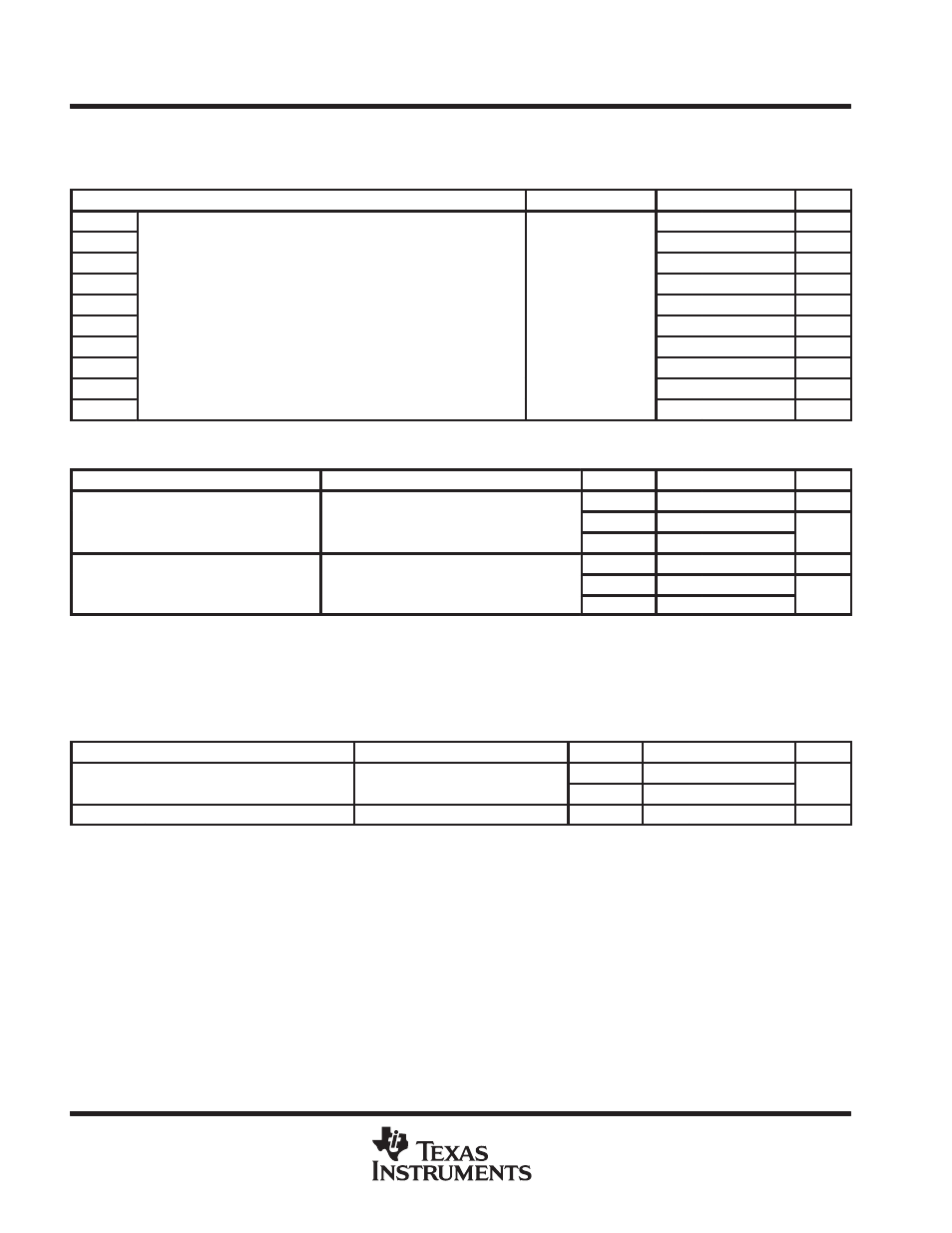
optional resistors, individually programmable with ROM code (see Note 13)
PARAMETER
TEST CONDITIONS
MIN
TYP
MAX
UNIT
R(opt1)
2.5
5
10
k
Ω
R(opt2)
3.8
7.7
15
k
Ω
R(opt3)
7.6
15
31
k
Ω
R(opt4)
11.5
23
46
k
Ω
R(opt5)
Resistors, individually programmable with ROM code, all port pins,
VCC = 2 2 V/3 V
23
45
90
k
Ω
R(opt6)
y
g
values applicable for pulldown and pullup
VCC = 2.2 V/3 V
46
90
180
k
Ω
R(opt7)
70
140
280
k
Ω
R(opt8)
115
230
460
k
Ω
R(opt9)
160
320
640
k
Ω
R(opt10)
205
420
830
k
Ω
NOTE 13: Optional resistors Roptx for pulldown or pullup are not available in standard flash memory device MSP430F11x1.
inputs Px.x, TAx
PARAMETER
TEST CONDITIONS
VCC
MIN
TYP
MAX
UNIT
Port P1, P2: P1.x to P2.x,
2.2 V/3 V
1.5
cycle
t(int)
External interrupt timing
Port P1, P2: P1.x to P2.x,
External trigger signal for the interrupt flag,
2.2 V
62
ns
(
)
(see Note 14)
3 V
50
ns
2.2 V/3 V
1.5
cycle
t(cap)
Timer_A, capture timing
TA0, TA1, TA2. (see Note 15)
2.2 V
62
ns
(
)
3 V
50
ns
NOTES: 14. The external signal sets the interrupt flag every time the minimum tint cycle and time parameters are met. It may be set even with
trigger signals shorter than tint. Both the cycle and timing specifications must be met to ensure the flag is set. tint is measured in MCLK
cycles.
15. The external capture signal triggers the capture event every time when the minimum tcap cycles and time parameters are met. A
capture may be triggered with capture signals even shorter than tcap. Both the cycle and timing specifications must be met to ensure
a correct capture of the 16-bit timer value and to ensure the flag is set.
internal signals TAx, SMCLK at Timer_A
PARAMETER
TEST CONDITIONS
VCC
MIN
TYP
MAX
UNIT
f(IN)
Input frequency
Internal TA0 TA1 TA2 tH = tL
2.2 V
8
MHz
f(IN)
Input frequency
Internal TA0, TA1, TA2, tH = tL
3 V
10
MHz
f(TAint)
Timer_A clock frequency
Internally, SMCLK signal applied
2.2 V/3 V
dc
fSystem