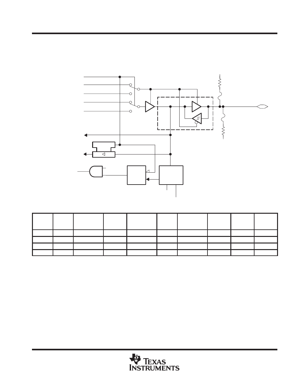
Application information input/output schematic – Texas Instruments MSP430x11x1 User Manual
Page 37

MSP430x11x1
MIXED SIGNAL MICROCONTROLLER
SLAS241C – SEPTEMBER 1999 – REVISED JUNE 2000
37
POST OFFICE BOX 655303
•
DALLAS, TEXAS 75265
APPLICATION INFORMATION
input/output schematic
Port P1, P1.0 to P1.3, input/output with Schmitt-trigger
EN
D
(See Note 27)
(See Note 28)
(See Note 28)
(See Note 27)
GND
VCC
P1.0 – P1.3
0
1
0
1
Interrupt
Edge
Select
EN
Set
Q
P1IE.x
P1IFG.x
P1IRQ.x
Interrupt
Flag
P1IES.x
P1SEL.x
Module X IN
P1IN.x
P1OUT.x
Module X OUT
Direction Control
From Module
P1DIR.x
P1SEL.x
Pad Logic
NOTE: x = Bit/identifier, 0 to 3 for port P1
PnSel.x
PnDIR.x
Direction
control from
module
PnOUT.x
Module X OUT
PnIN.x
Module X IN
PnIE.x
PnIFG.x
PnIES.x
P1Sel.0
P1DIR.0
P1DIR.0
P1OUT.0
VSS
P1IN.0
TACLK†
P1IE.0
P1IFG.0
P1IES.0
P1Sel.1
P1DIR.1
P1DIR.1
P1OUT.1
Out0 signal†
P1IN.1
CCI0A†
P1IE.1
P1IFG.1
P1IES.1
P1Sel.2
P1DIR.2
P1DIR.2
P1OUT.2
Out1 signal†
P1IN.2
CCI1A†
P1IE.2
P1IFG.2
P1IES.2
P1Sel.3
P1DIR.3
P1DIR.3
P1OUT.3
Out2 signal†
P1IN.3
CCI2A†
P1IE.3
P1IFG.3
P1IES.3
† Signal from or to Timer_A
NOTES: 27. Optional selection of pullup or pulldown resistors with ROM (masked) versions.
28. Fuses for optional pullup and pulldown resistors can only be programmed at the factory (ROM versions only).
