Texas Instruments MSP430x11x1 User Manual
Page 12
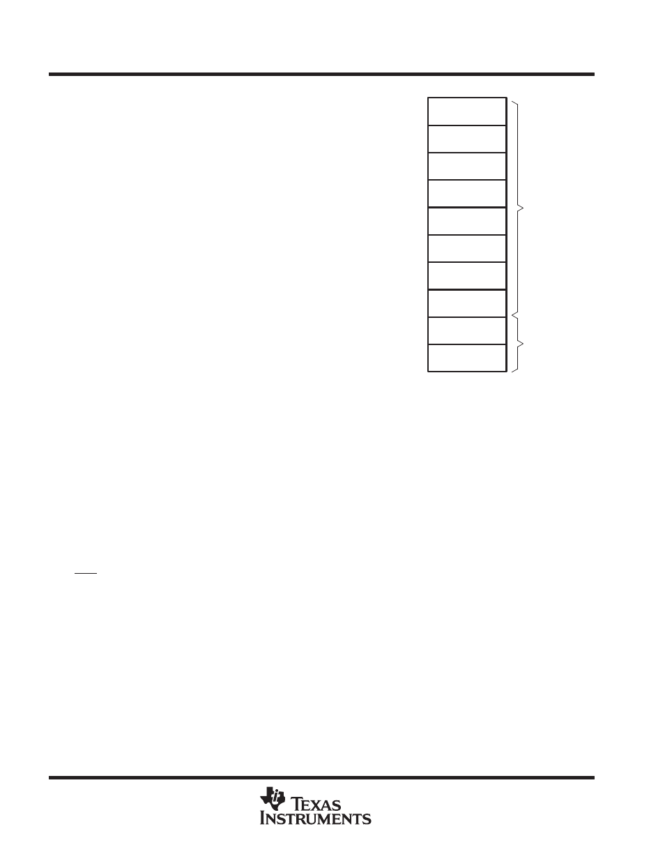
Segment0 w/
Interrupt Vectors
0FFFFh
0FE00h
Information
Memory
Flash Main Memory
Segment1
Segment2
Segment3
Segment4
Segment5
Segment6
Segment7
SegmentA
SegmentB
0FDFFh
0FC00h
0FBFFh
0FA00h
0F9FFh
0F800h
0F7FFh
0F600h
0F5FFh
0F400h
0F3FFh
0F200h
0F1FFh
0F000h
010FFh
01080h
0107Fh
01000h
NOTE: All segments not implemented on all devices.
MSP430x11x1
MIXED SIGNAL MICROCONTROLLER
SLAS241C – SEPTEMBER 1999 – REVISED JUNE 2000
12
POST OFFICE BOX 655303
•
DALLAS, TEXAS 75265
flash memory
The flash memory consists of 512-byte segments
in the main memory and 128-byte segments in the
information memory. See device memory maps
for specific device information.
Segment0 to Segment7 can be erased
individually, or altogether as a group.
SegmentA and SegmentB can be erased
individually, or as a group with segments 0–7.
The memory in SegmentA and SegmentB is also
called
Information Memory.
VPP is generated internally. VCC current
increases during programming.
During program/erase cycles, VCC must not drop
below the minimum specified for program/erase
operation.
Program and erase timings are controlled by the
flash timing generator—no software intervention
is needed. The input frequency of the flash timing
generator should be in the proper range and must
be applied until the write/program or erase
operation is completed.
During program or erase, no code can be executed from flash memory and all interrupts must be disabled by
setting the GIE, NMIE, ACCVIE, and OFIE bits to zero. If a user program requires execution concurrent with
a flash program or erase operation, the program must be executed from memory other than the flash memory
(e.g., boot ROM, RAM). In the event a flash program or erase operation is initiated while the program counter
is pointing to the flash memory, the CPU will execute JMP $ instructions until the flash program or erase
operation is completed. Normal execution of the previously running software then resumes.
Unprogrammed, new devices may have some bytes programmed in the information memory (needed for test
during manufacturing). The user should perform an erase of the information memory prior to first use.
flash memory control register FCTL1
All control bits are reset during PUC. PUC is active after V
CC
is applied, a reset condition is applied to the
RST/NMI pin, the watchdog timer expires, a watchdog access violation occurs, or an improper flash operation
has been performed. A more detailed description of the control-bit functions is found in the flash memory module
description (refer to
MSP430x1xx User’s Guide, literature number SLAU049). Any write to control register
FCTL1 during erase, mass erase, or write (programming) will end in an access violation with ACCVIFG=1.
Special conditions apply for segment-write mode. Refer to
MSP430x1xx User’s Guide, literature number
SLAU049 for details.