Application information – Texas Instruments MSP430x11x1 User Manual
Page 38
MSP430x11x1
MIXED SIGNAL MICROCONTROLLER
SLAS241C – SEPTEMBER 1999 – REVISED JUNE 2000
38
POST OFFICE BOX 655303
•
DALLAS, TEXAS 75265
APPLICATION INFORMATION
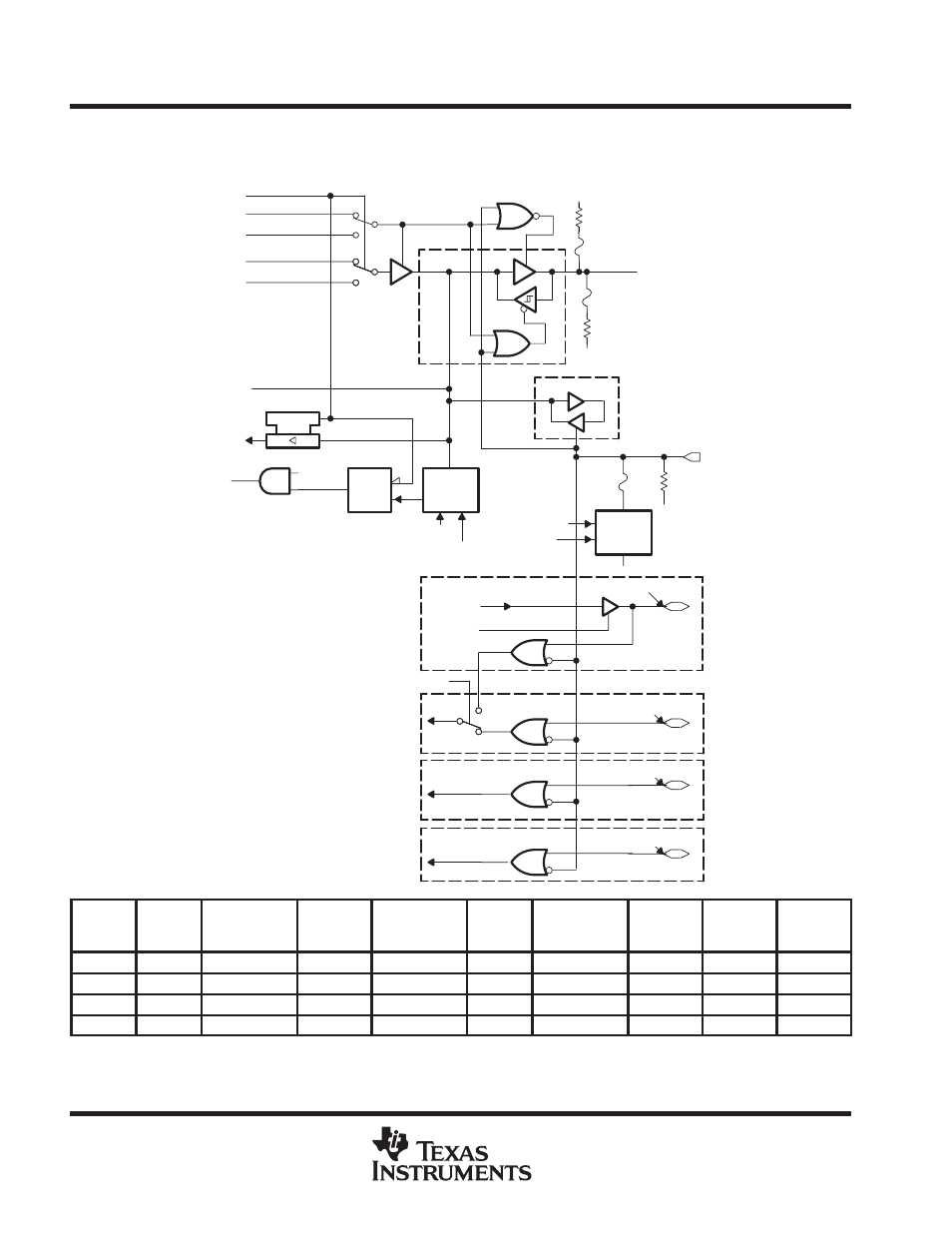
Port P1, P1.4 to P1.7, input/output with Schmitt-trigger and in-system access features
EN
D
See Note 27
See Note 28
See Note 28
See Note 27
GND
VCC
P1.4–P1.7
0
1
0
1
Interrupt
Edge
Select
EN
Set
Q
P1IE.x
P1IFG.x
P1IRQ.x
Interrupt
Flag
P1IES.x
P1SEL.x
Module X IN
P1IN.x
P1OUT.x
Module X OUT
Direction Control
From Module
P1DIR.x
P1SEL.x
Pad Logic
Bus Keeper
TST
Fuse
60 k
Ω
Fuse
Blow
Control
Control By JTAG
0
1
TDO
Controlled By JTAG
P1.x
TDI
P1.x
TST
TST
TMS
TST
TCK
TST
Controlled by JTAG
TST
P1.x
P1.x
NOTE: The test pin should be protected from potential EMI
and ESD voltage spikes. This may require a smaller
external pulldown resistor in some applications.
x = Bit identifier, 4 to 7 for port P1
During programming activity and during blowing
the fuse, the pin TDO/TDI is used to apply the test
input for JTAG circuitry.
P1.7/TDI/TDO
P1.6/TDI
P1.5/TMS
P1.4/TCK
Typical
TEST
GND
NOTE: Fuse not implemented
in F11x1
PnSel.x
PnDIR.x
Direction
control from
module
PnOUT.x
Module X OUT
PnIN.x
Module X IN
PnIE.x
PnIFG.x
PnIES.x
P1Sel.4
P1DIR.4
P1DIR.4
P1OUT.4
SMCLK
P1IN.4
unused
P1IE.4
P1IFG.4
P1IES.4
P1Sel.5
P1DIR.5
P1DIR.5
P1OUT.5
Out0 signal†
P1IN.5
unused
P1IE.5
P1IFG.5
P1IES.5
P1Sel.6
P1DIR.6
P1DIR.6
P1OUT.6
Out1 signal†
P1IN.6
unused
P1IE.6
P1IFG.6
P1IES.6
P1Sel.7
P1DIR.7
P1DIR.7
P1OUT.7
Out2 signal†
P1IN.7
unused
P1IE.7
P1IFG.7
P1IES.7
† Signal from or to Timer_A
NOTES: 27. Optional selection of pullup or pulldown resistors with ROM (masked) versions.
28. Fuses for optional pullup and pulldown resistors can only be programmed at the factory (ROM versions only).