Texas Instruments MSP430x11x1 User Manual
Page 13
MSP430x11x1
MIXED SIGNAL MICROCONTROLLER
SLAS241C – SEPTEMBER 1999 – REVISED JUNE 2000
13
POST OFFICE BOX 655303
•
DALLAS, TEXAS 75265
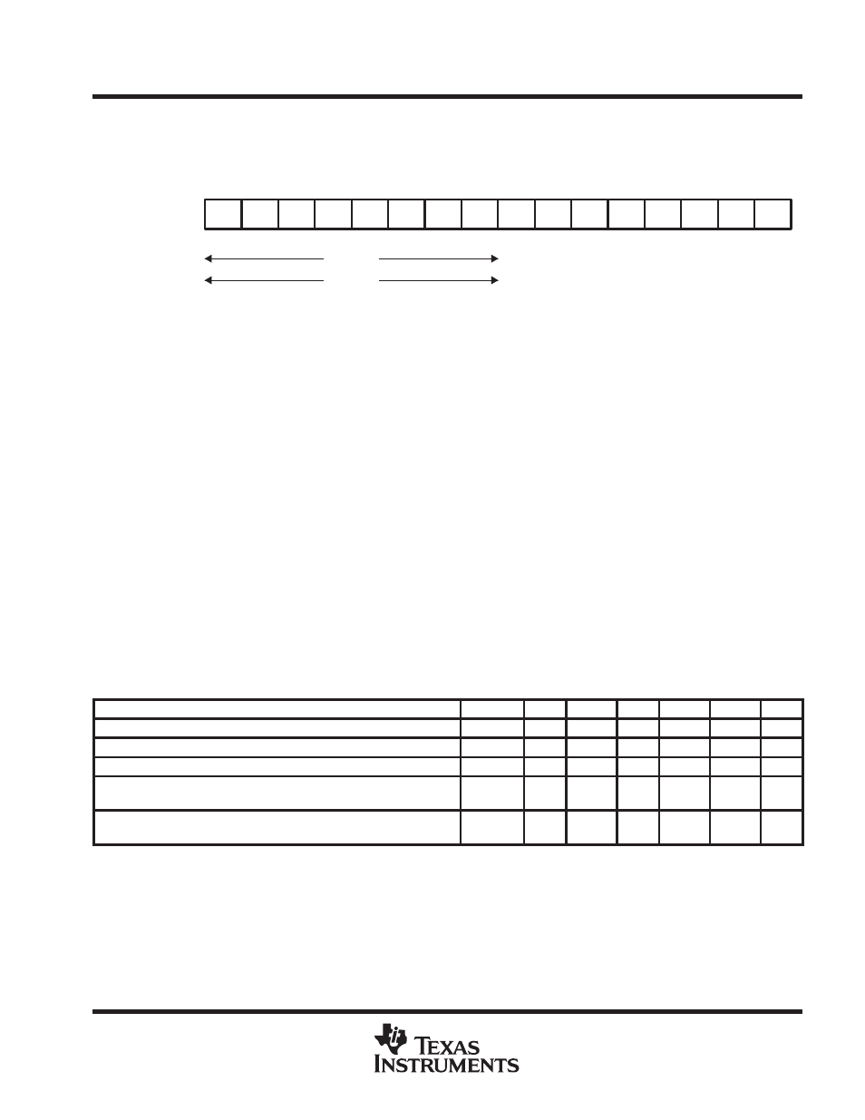
flash memory control register FCTL1 (continued)
Read access is possible at any time without restrictions.
The control bits of control register FCTL1 are:
SEG
WRT
FCTL1
0128h
MEras
Erase
res.
0
r0
rw-0
rw–0
7
rw–0
WRT
rw–0
res.
r0
res.
r0
res.
r0
8
15
FCTL1 read:
096h
FCTL1 write:
0A5h
Erase
0128h, bit1,
Erase a segment
0:
1:
No segment erase will be started.
Erase of one segment is enabled. The segment to be erased is defined by a
dummy write into any address within the segment. The erase bit is
automatically reset when the erase operation is completed.
MEras
0128h, bit2,
Mass Erase, main memory segments are erased together.
0:
1:
No segment erase will be started.
Erase of main memory segments is enabled. Erase starts when a dummy
write to any address in main memory is executed. The MEras bit is
automatically reset when the erase operation is completed.
WRT
0128h, bit6,
Bit WRT must be set for a successful write execution.
If bit WRT is reset and write access to the flash memory is attempted, an
access violation occurs and ACVIFG is set.
SEGWRT
0128h, bit7,
Bit SEGWRT may be used to reduce total programming time.
Refer to
MSP430x1xx User’s Guide, literature number SLAU049 for details.
0:
1:
No segment-write acceleration is selected.
Segment-write is used. This bit needs to be reset and set between segment
borders.
Table 3. Allowed Combinations of Control Bits Allowed for Flash Memory Access
FUNCTION PERFORMED
SEGWRT
WRT
MEras
Erase
BUSY
WAIT
Lock
Write word or byte
0
1
0
0
0
0
0
Write word or byte in same segment, segment write mode
1
1
0
0
0
→
1
0
→
1
0
Erase one segment by writing to any address in the target segment
0
0
0
1
0
0
0
Erase all segments (0 to 7) but not the information memory
(segments A and B)
0
0
1
0
0
0
0
Erase all segments (0 to 7 and A and B) by writing to any address in
the flash memory module
0
0
1
1
0
0
0
NOTE: The table shows all valid combinations. Any other combination will result in an access violation.
flash memory, timing generator, control register FCTL2
The timing generator (Figure 1) generates all the timing signals necessary for write, erase, and mass erase from
the selected clock source. One of three different clock sources may be selected by control bits SSEL0 and
SSEL1 in control register FCTL2. The selected clock source should be divided to meet the frequency
requirements specified in the recommended operating conditions.