5 pci interface timing, Table 7.16 pci timing, Pci interface timing – LSI 53C810A User Manual
Page 208: Pci timing, Section 7.5, “pci interface timing
7-26
Electrical Characteristics
7.5 PCI Interface Timing
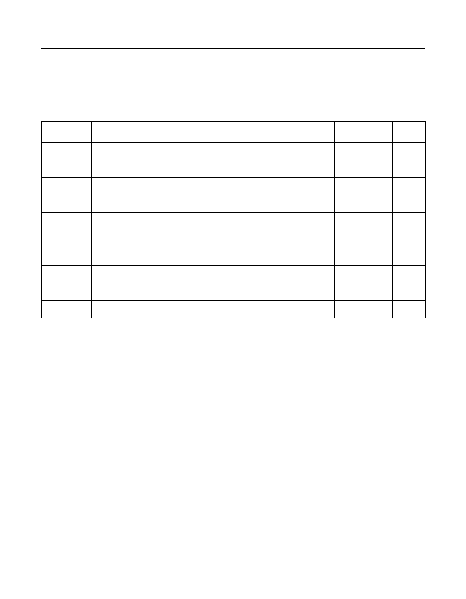
describes the PCI timing data for the LSI53C810A.
Table 7.16
PCI Timing
Symbol
Parameter
Min
Max
Unit
t
1
Shared signal input setup time
7
–
ns
t
2
Shared signal input hold time
–
–
ns
t
3
CLK to shared signal output valid
–
11
ns
t
4
Side signal input setup time
10
–
ns
t
5
Side signal input hold time
–
–
ns
t
6
CLK to side signal output valid
–
12
ns
t
7
CLK high to FETCH/ low
–
20
ns
t
8
CLK high to FETCH/ high
–
20
ns
t
9
CLK high to MASTER/ low
–
20
ns
t
10
CLK high to MASTER/ high
–
20
ns