Figure6.4 read/write register instruction, Read/write register instruction – LSI 53C810A User Manual
Page 165

Read/Write Instructions
6-25
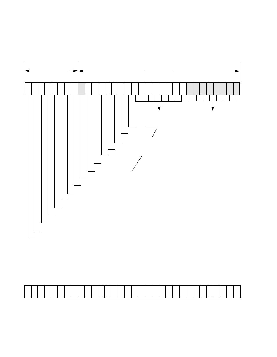
illustrates the register bit values that represent a Read/Write
instruction.
Figure 6.4
Read/Write Register Instruction
31 30 29 28 27 26 25 24 23 22 21 20 19 18 17 16 15 14 13 12 11 10 9
8
7
6
5
4
3
2
1
0
31 30 29 28 27 26 25 24 23 22 21 20 19 18 17 16 15 14 13 12 11 10 9
8
7
6
5
4
3
2
1
0
DSPS Register
DCMD Register
DBC Register
A0
A1
A2
A3
A4
A5
A6
0 (Reserved)
Operator 0
Operator 1
Operator 2
Opcode Bit 0
Opcode Bit 1
Opcode Bit 2
1 - Instruction Type - R/W
0 - Instruction Type - R/W
Immediate Data
Reserved (must be 0)
Register
Address
