18 warm reset register (wrr), 20 spi address register (sar), Ction 4.2.18), res – SBE HighWire HW400c/2 User Manual
Page 70
HighWire HW400c/2 User Reference Guide Rev 1.0
4.2.18 Warm Reset Register (WRR)
The Warm Reset Register is a Read/Write Register. Writing a value of 0x77 to the
Warm Reset Register initializes a Warm Reset. The actual reset signal is driven by
the CPLD 1-2 milliseconds after writing 0x77 to the WRR. The CPU, System
Controller, CPLD registers, T8110, Disk on Chip, Ethernet Switch and PHYs, and
local PCI (PCI1) are all reset. Host PCI (PCI0) reset is not affected. Writing a value
ther than 0x77 to the WRR has no effect, except the value is latched and readable.
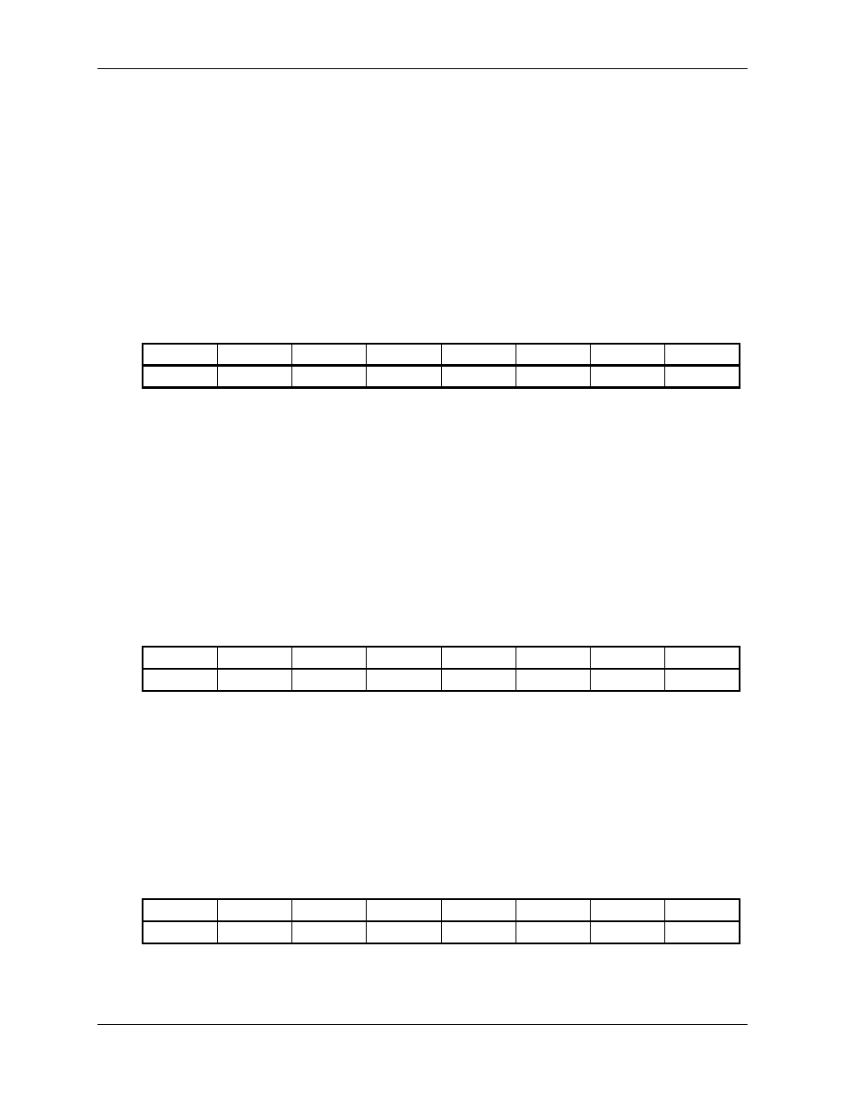
Table 48. Warm Reset Register (WRR) Offset address 0x17
Bit 7
Bit 6
Bit 5
Bit 4
Bit 3
Bit 2
Bit 1
Bit 0
o
W
W
W
W
W
W
W
W
RR7 RR6 RR5 RR4 RR3 RR2 RR1 RR0
WRR[7:0]
= 0x77
Warm reset
hed
4.2.19 SPI Page
egister (SP
he SPI Page Register is a Read/Write register. It is used for selecting the desired
age when accessing the BCM5388 Ethernet Switch SPI port.
ister (SPR) Offset Address 0x1A
Bit 7
WRR[7:0]
≠ 0x77
No effect, value is latc
R
R)
T
p
Table 49. SPI Page Reg
Bit 6
Bit 5
Bit 4
Bit 3
Bit 2
Bit 1
Bit 0
SPR7
PR0
SPR6 SPR5 SPR4 SPR3 SPR2 SPR1 S
SPR[7:0]
= 0x00 – 0xFF
4.2.20 SPI Addre
Th
Addre
ad/W
ister.
sed fo
ting t
red
whe
ssing
M53
ernet
50.
Re
Bit 7
Bit 6
Bit 5
Bit 4
Bit 3
Bit 2
Bit 1
Bit 0
ss Register (SAR)
e SPI
ss Register is a Re
rite reg
n acce
It is u
the BC
r selec
88 Eth
he desi
Switch
register address (within each page)
SPI port.
Table
SPI Address
gister (SAR) Offset Address 0x1B
SAR7 SAR6 SAR5 SAR4 SAR3 SAR2 SAR1 SAR0
SPR[7:0]
= 0x00 – 0xFF
October 10, 2006
Copyright 2006, SBE, Inc.
Page
58