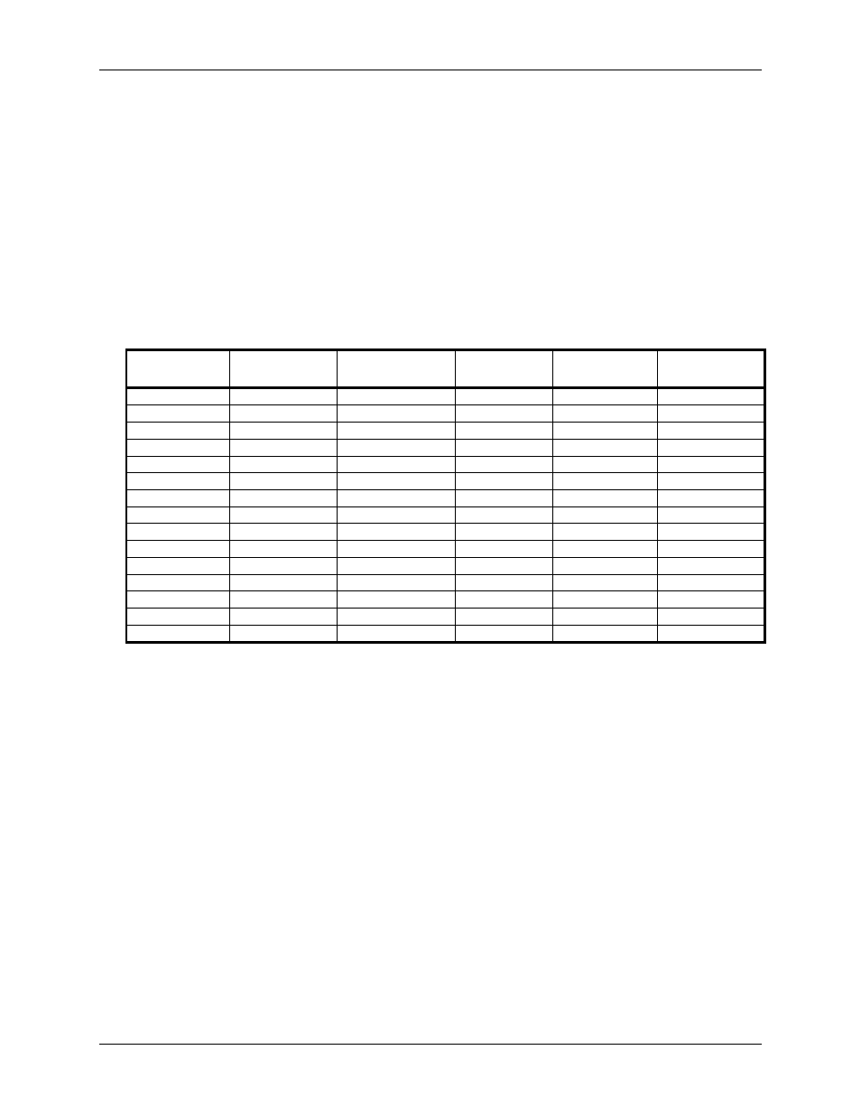
Programming information, 1 hw400c/2 memory map, Table 28. hw400c/2 memory map – SBE HighWire HW400c/2 User Manual
Page 58
HighWire HW400c/2 User Reference Guide Rev 1.0
4
PROGRAMMING INFORMATION
mmable register information is provided in
is section.
.1 HW400c/2 M
Table 28 shows the m
2 board.
Table 28. HW400c/2 Memory Ma
Address
Start (Hex)
re
d (H
Device No.
Device Size
y
Size
The HW400c/2 memory map and progra
th
4
emory Map
emory map for the HW400c/
p
Add ss
En
ex)
Device
Memor
Window
0
F F
256MB Mem0/Mem1
6 MB
0FF
FFF
SDRAM
25
256 MB
0
F F
Mem0/Mem1
2 MB
B
1FF
FFF
SDRAM 512MB
51
512 M
0
F F
0/Mem1
GB
3FF
FFF
SDRAM 1GB
Mem
1
1 GB
0
F F
Mem0/Mem1
GB
7FF
FFF
SDRAM 2GB
2
2 GB
E000 0000
F
– 8GB
E000 FFF
Disk-on-Chip
Dev 0
128MB
64 KB
E100 0000
00 F
Dev 1
E1
FFF
CPLD
< 100 Bytes
64 KB
E200 0000
0F F
Dev 2
E2
FFF
T8110L
1 MB
F100 0000
00 F
F1
FFF
MV64462 Reg
64 KB
F100 0850
MV64462 Timer
F100 8000
MV64462 UART
FF00 0000
F F
om
Dev 3
2 KB
FF7
FFF
Boot R
51
8 MB
FF80 0000
FF F
Dev Boot
2 KB
FF
FFF
Boot SRAM
51
8 MB
October 10, 2006
Copyright 2006, SBE, Inc.
Page
46