Block diagram, Chapter 1: introduction, Rohs 6/6 – SUPER MICRO Computer X8SIL User Manual
Page 17: Ddr3 (cha), Pcie2.0_x8, Vrm 11.1, Ddr3 (chb), Misc vrs, Pcie_x4, Pci 32
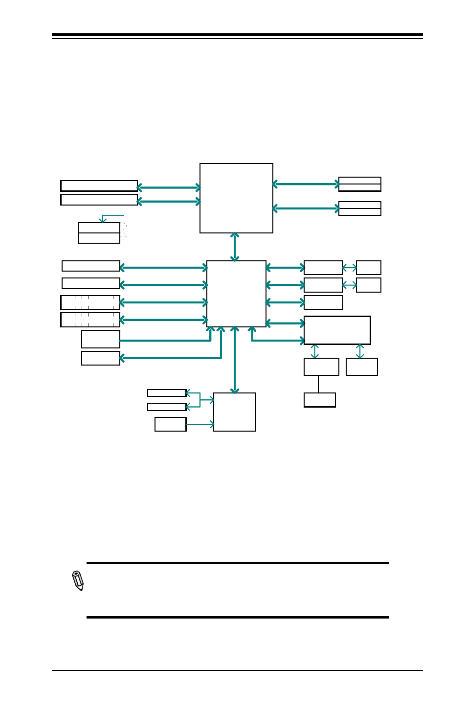
Chapter 1: Introduction
1-9
X8SIL / X8SIL-F System Block Diagram
Note: This is a general block diagram and may not exactly represent
the features on your motherboard. See the Motherboard Features
pages for the actual specifications of each motherboard.
5
5
4
4
3
3
2
2
1
1
D
D
C
C
B
B
A
A
Title
Size
Document Number
Rev
Date:
Sheet
of
S
UPERMICR
980 Rock Ave. San Jose, CA 95131, USA
TEL:408-503-8000
CONFIDENTIAL- DO NOT DUPLICATE
BLOCK DIGRAM
1.01
X8SIL
C
2
36
Wednesday, July 29, 2009
Title
Size
Document Number
Rev
Date:
Sheet
of
S
UPERMICR
980 Rock Ave. San Jose, CA 95131, USA
TEL:408-503-8000
CONFIDENTIAL- DO NOT DUPLICATE
BLOCK DIGRAM
1.01
X8SIL
C
2
36
Wednesday, July 29, 2009
Title
Size
Document Number
Rev
Date:
Sheet
of
S
UPERMICR
980 Rock Ave. San Jose, CA 95131, USA
TEL:408-503-8000
CONFIDENTIAL- DO NOT DUPLICATE
BLOCK DIGRAM
1.01
X8SIL
C
2
36
Wednesday, July 29, 2009
Clarkdale
IBexPeak
BLOCK DIAGRAM
DDR3 (CHA)
(Lynnfield)
PCIe2.0_x8
JI2C1
I2C bus for PCI Slot
JI2C2
DISABLE
ENABLE
CLOSE CLOSE
Enable
Disable
JPL1
Gb_LAN 1
2-3
JBT1
Normal
Clear
Clear CMOS
3-4
SPEAKER
SPK_HEADER
Internal_Buzzer
External_Speaker
BUZZER/SPEAKER
LE1: STBY Warning LED
OPEN
JPF
CLOSE
DISABLE
ENABLE
PWR_FORCE_ON
OPEN
OPEN
1-2
PCI-32 AD16
PIRQ E F G H
PREQ_0
PCLK3
JPUSB1
B/P USB
Wake-up
VRM 11.1
VID[0-7]
RoHS 6/6
LPC I/O
W83627DHG
1-2
Enable
Disable
2-3
PCIe x8 SLOT
RJ45
RJ45
DDR3 (CHB)
DIMM1(Far)
DIMM2
DIMM1(Far)
DIMM2
4 UDIMM
MISC VRs
1333/1066MHz
1333/1066MHz
5.0Gb
x4
D
MI
2.
5G
b
PCH
2.5Gbps
PCIe_x4
PCIe x8 SLOT
PCI 32
1 PCI 32 SLOT
4/6 SATA PORTS
SATA-II
300MB/s
5/7 USB PORTS
USB2.0
480Mbps
FLASH
SPI 16Mb
SPI
PCIe_x1
2.5Gbps
GLAN1
82574L
CK505
Rev1.0
CLOCK
COM1,2
P/S2
LPC
HEALTH
INFO
P5-8
P10
P11-14
P12
P4
P15
P20
LPC
TPM1.2
P15
P28-29
P9
P23
P21
P21
JPT1
1-3
Enable
Disable
2-4
TPM
LPC
PCIe_x1
2.5Gbps
2-3
Gb_LAN 2
JPL2
Disable
Enable
1-2
Based on customer spec
1-2
2-3
PCIe2.0_x8
PCIe x8 SLOT
5.0Gb
Intel 3400/3420
GLAN2
82574L
RMII
VGA
PORT
RTL8201N
PHY
RJ45
HERMON WPCM450
WINBOND
PCI32
P26-27
P18
P19
P18
P19
P16
P17
P30-32
P33
P34
P33
Hermon AD19
PIRQ H
PREQ_3
PCLK0,1
Enable
Disable
JPG1
VGA
2-3
1-2
(HERMON)
Enable
Disable
JPB
BMC
2-3
1-2
Xeon 3400 Series
4 RDIMM
(4 Quad rank
RDIMM run on
800MHz)
Note:
ES1 Lynnfield (A0 stepping Q1XX) can not be used on the board;
ES2 Lynnfield (A1 stepping Q2XX) need to uninstall R52, R53;
QS Lynnfield (B1 stepping Q3XX) or later can be used.
All Clarkdale samples or later can be used.
(option)