Lcon — lcd control register, Lcon – Samsung S3C8275X User Manual
Page 90
CONTROL REGISTERS
S3C8275X/F8275X/C8278X/F8278X/C8274X/F8274X
4-20
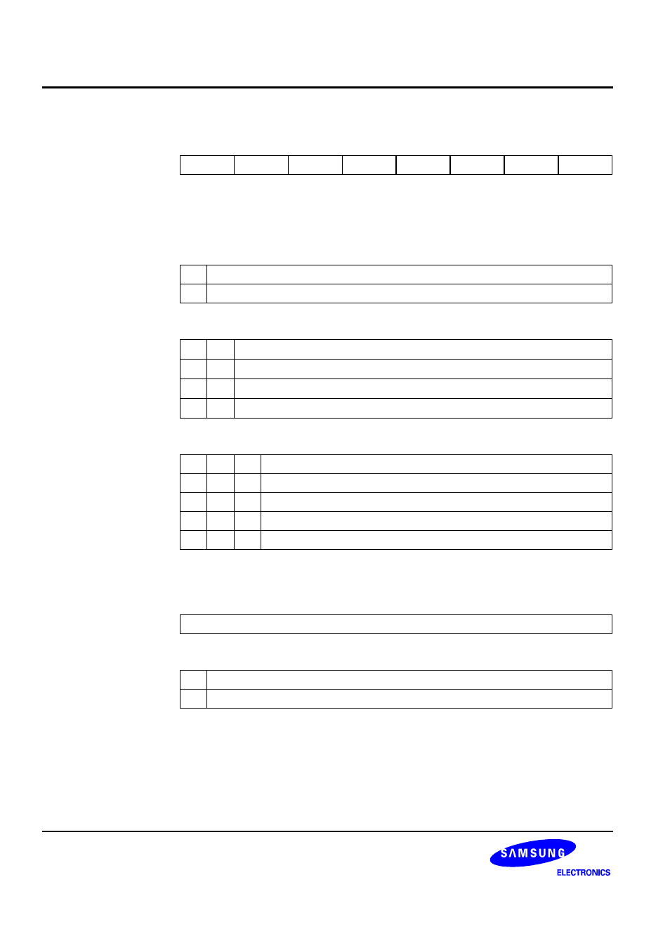
LCON
— LCD Control Register
E0H
Set 1, Bank 1
Bit
Identifier
.7 .6 .5 .4 .3 .2 .1 .0
Reset Value
0 0 0 0 0 0 – 0
Read/Write
R/W R/W R/W R/W R/W
R/W – R/W
Addressing Mode
Register addressing mode only
.7
Internal LCD Dividing Resistors Enable Bit
0
Enable internal LCD dividing resistors
1
Disable internal LCD dividing resistors
.6–.5
LCD Clock Selection Bits
0 0
fw/2
9
(64 Hz)
0 1
fw/2
8
(128 Hz)
1 0
fw/2
7
(256 Hz)
1 1
fw/2
6
(512 Hz)
.4–.2
LCD Duty and Bias Selection Bits
0 0 0
1/4duty,
1/3bias
0 0 1
1/3duty,
1/3bias
0 1 0
1/3duty,
1/2bias
0 1 1
1/2duty,
1/2bias
1 x x
Static
NOTES:
1. "x" means don't care.
2. When 1/2 bias is selected, the bias levels are set as V
LC0
, V
LC1
(V
LC2
), and V
SS
.
.1
Not used for the S3C8275X/C8278X/C8274X
.0
LCD Display Control Bit
0
Turn display off (Turn off the P-Tr)
1
Turn display on (Turn on the P-Tr)