Samsung S3C8275X User Manual
Page 29
S3C8275X/F8275X/C8278X/F8278X/C8274X/F8274X
PRODUCT
OVERVIEW
1-7
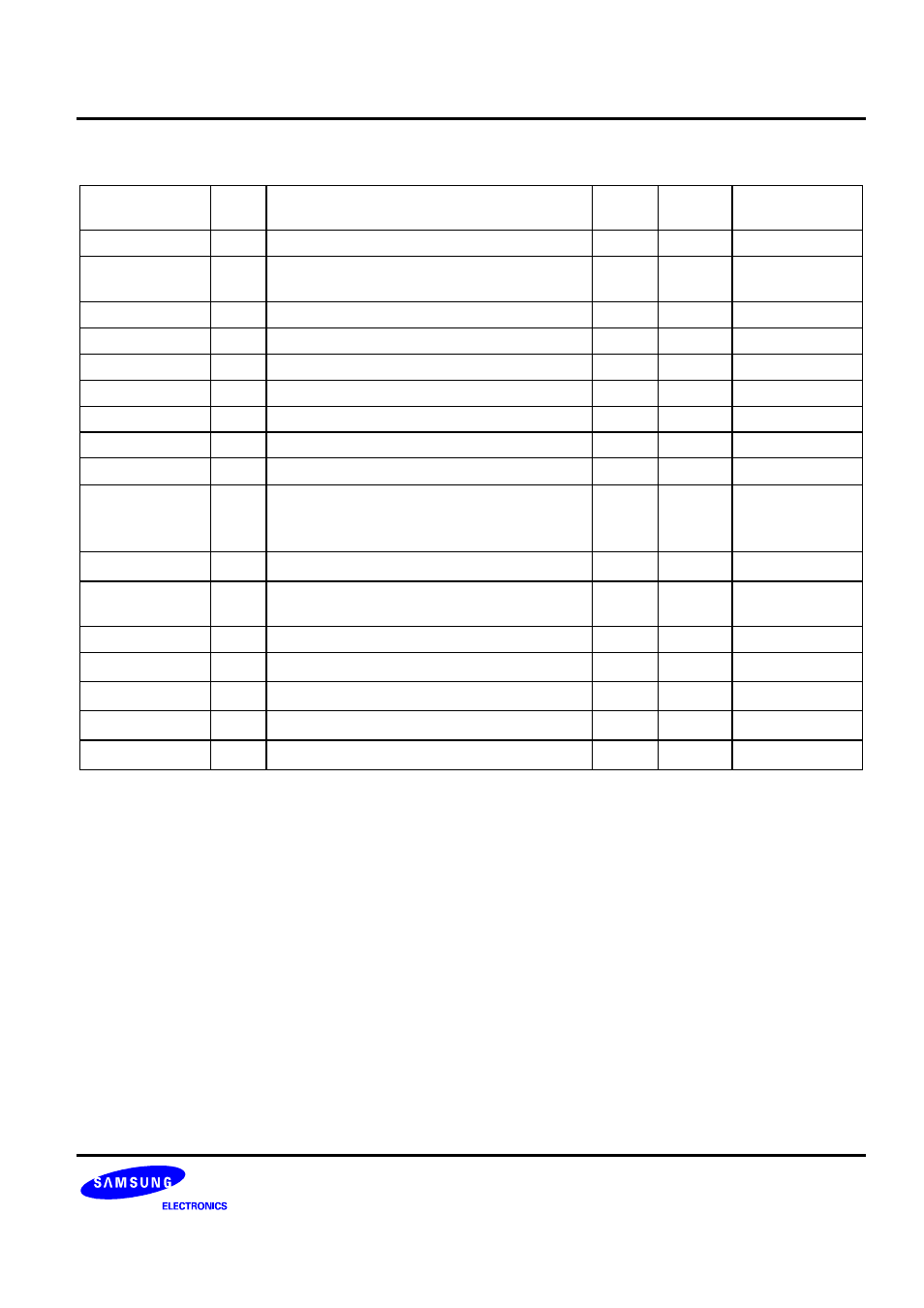
Table 1-1. S3C8275X/F8275X/C8278X/F8278X/C8274X/F8274X Pin Descriptions (Continued)
Pin
Names
Pin
Type
Pin
Description
Circuit
Type
Pin
No.
Shared
Functions
VLC0
−VLC2
−
LCD power supply pins.
−
6
−8
−
INT0
−INT2
INT3
−INT7
I/O
External interrupts input pins.
E-4
18
−20
29
−33
P0.0
−P0.2
P1.3
−P1.7
T1CLK
I/O
Timer 1/A external clock input.
E-4
21
P0.3
TAOUT
I/O
Timer 1/A clock output.
E-4
22
P0.4
TBOUT
I/O
Timer B clock output.
E-4
23
P0.5
CLKOUT
I/O
System clock output.
E-4
24
P0.6
BUZ
I/O
Output pin for buzzer signal.
E-4
25
P0.7
SCK, SO, SI
I/O
Serial clock, data output, and data input.
E-4
26,27,28 P1.0, P1.1, P1.2
COM0–COM3
I/O
LCD common signal outputs.
H-9
2
−5 P6.0−P6.3
SEG0–SEG15
SEG16–SEG30
SEG31
I/O
LCD segment signal outputs.
H-9
H-8
H-10
1,64
− 50
49
−35
34
P5.7
−P4.0
P3.7
−P2.1
P2.0/V
BLDREF
V
BLDREF
I/O
Battery level detector reference voltage
H-10
34
P2.0/SEG31
V
REG
O
Regulator voltage output for sub clock
(needed 0.1uF)
−
17
−
nRESET
I
System reset pin
B
16
−
XT
IN
, XT
OUT
−
Sub oscillator pins
−
14, 15
−
X
IN
, X
OUT
−
Main oscillator pins.
−
12, 11
−
TEST I
Test input: it must be connected to V
SS
−
13
−
V
DD
, V
SS
−
Power input pins
−
9, 10
−