Table 17-4. input/output capacitance – Samsung S3C8275X User Manual
Page 301
ELECTRICAL DATA
S3C8275X/F8275X/C8278X/F8278X/C8274X/F8274X
17-6
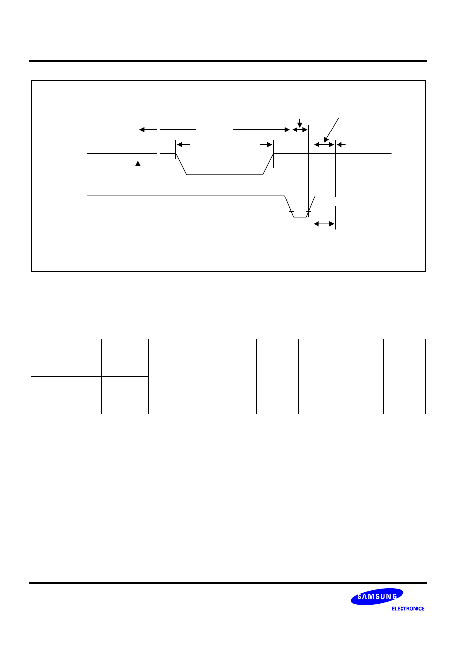
Execution of
STOP Instrction
RESET
Occurs
~ ~
V
DDDR
~ ~
Stop Mode
Oscillation
Stabilization
TIme
Normal
Operating Mode
Data Retention Mode
t
WAIT
nRESET
V
DD
0.2 V
DD
0.8 V
DD
NOTE:
t
WAIT
is the same as 16
× 1/BT clock.
Figure 17-2. Stop Mode Release Timing When Initiated by a RESET
Table 17-4. Input/Output Capacitance
(T
A
=
−25
°
C ~ + 85
°
C, V
DD
=
0 V)
Parameter Symbol
Conditions
Min Typ Max Unit
Input
capacitance
C
IN
f = 1 MHz; unmeasured pins
are connected to V
SS
−
−
10 pF
Output
capacitance
C
OUT
I/O capacitance
C
IO