Pin descriptions – Samsung S3C8275X User Manual
Page 28
PRODUCT OVERVIEW
S3C8275X/F8275X/C8278X/F8278X/C8274X/F8274X
1
-6
PIN DESCRIPTIONS
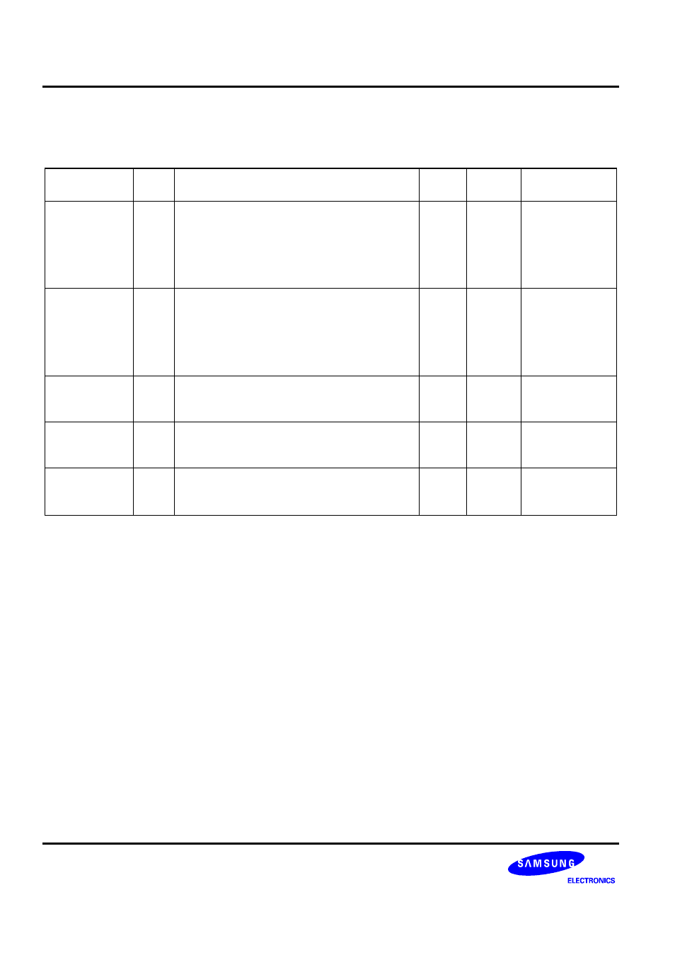
Table 1-1. S3C8275X/F8275X/C8278X/F8278X/C8274X/F8274X Pin Descriptions
Pin
Names
Pin
Type
Pin
Description
Circuit
Type
Pin
No.
Shared
Functions
P0.0
−P0.2
P0.3
P0.4
P0.5
P0.6
P0.7
I/O
I/O port with bit-programmable pins;
Schmitt trigger input or push-pull, open-drain
output and software assignable pull-ups;
P0.0
−P0.2 are alternately used for external
interrupt input(noise filters, interrupt enable
and pending control).
E-4
18
−20
21
22
23
24
25
INT0
−INT2
T1CLK
TAOUT
TBOUT
CLKOUT
BUZ
P1.0
P1.1
P1.2
P1.3
−P1.7
I/O
I/O port with bit-programmable pins;
Schmitt trigger input or push-pull, open-drain
output and software assignable pull-ups;
P1.3
−P1.7 are alternately used for external
interrupt input(noise filters, interrupt enable
and pending control).
E-4 26
27
28
29
−33
SCK
SO
SI
INT3
−INT7
P2.0
P2.1
−P2.7
I/O
I/O port with bit-programmable pins;
Input or push-pull, open-drain output and
software assignable pull-ups.
H-10
H-8
34
35
−41
SEG31/V
BLDREF
SEG30
−SEG24
P3.0
−P3.7
I/O
I/O port with bit-programmable pins;
Input or push-pull, open-drain output and
software assignable pull-ups.
H-8
42
−49 SEG23−SEG16
P4.0
−P4.7
P5.0
−P5.7
P6.0
−P6.3
I/O
I/O port with bit-programmable pins;
Input or push-pull output and software
assignable pull-ups.
H-9
50
−57
58
−64, 1
2
−5
SEG15
−SEG8
SEG7
−SEG0
COM0
−COM3