Input and output circuits, Iris video output, Trigger input – JAI AD-081GE User Manual
Page 12: Een (exposure enable) output, Ad-081ge, 11 fig.6 trigger circuit
AD-081GE
11
Fig.6 Trigger circuit
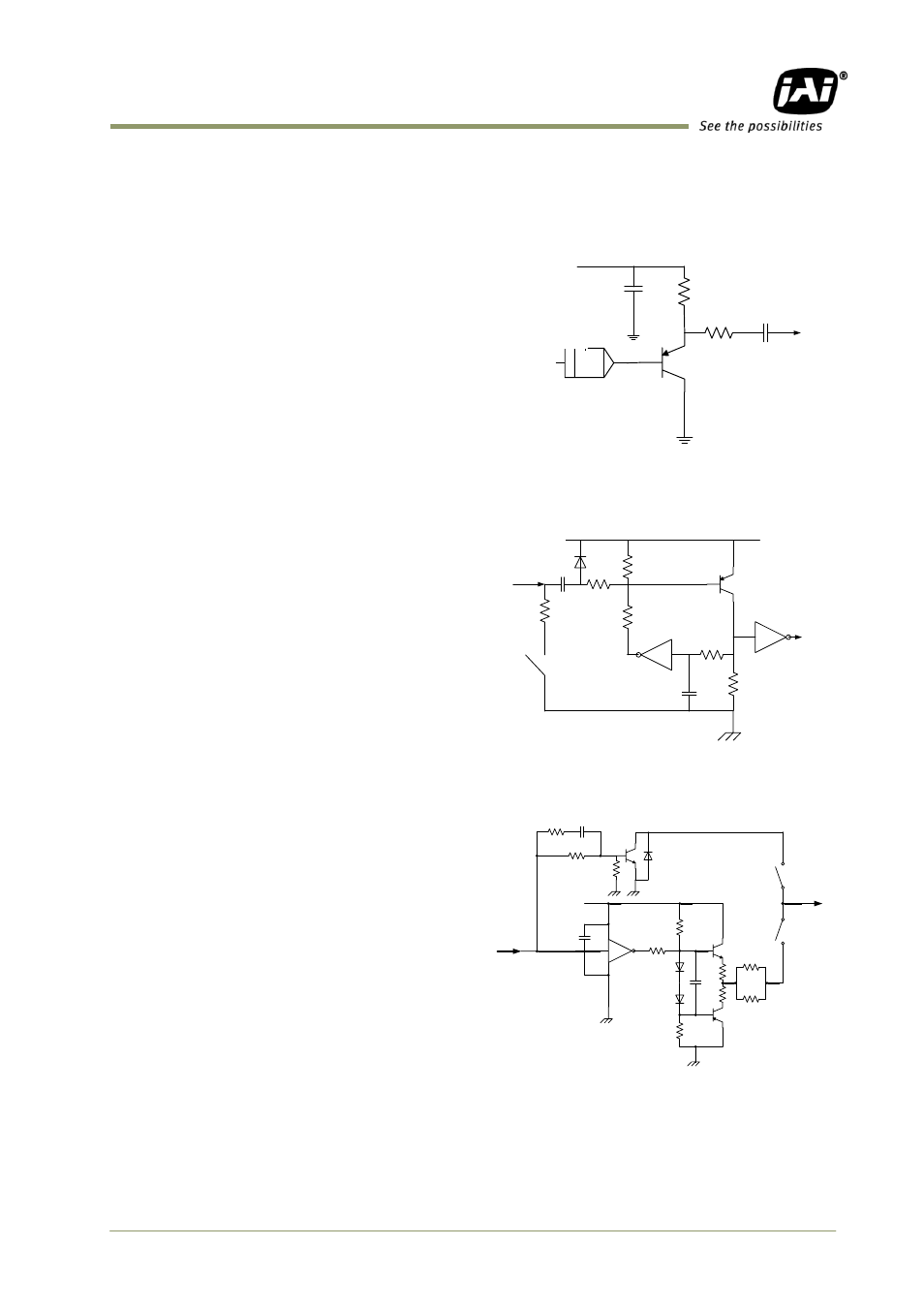
6. Input and output circuits
In the following schematic diagrams the input and output circuits for video and timing signals
are shown.
6.1. Iris Video output
This signal can be used for lens iris control in Continuous
mode. The signal is taken from the CCD sensor output
through the process circuit but as the reverse
compensation is applied, the signal is not influenced by
the gain settings. The video output is without sync. The
signal is 0.7 V p-p from 75
without termination.
This signal is taken from sensor 1 but it can be changed
by the register. In order to get this signal, DIP switch
DSW700 should be changed. Refer to 5.4.3.
Fig.5 Iris video output
6.2. Trigger input
An external trigger input can be applied to
pins 3 and 5 of the 6-pin Hirose connector.
The input is AC coupled. To allow long pulses
the input circuit is designed as a flip-flop
circuit. The leading and trailing edges of the
trigger pulse activate the circuit.
The trigger polarity can be changed.
Trigger input level 4 V
2 V.
6.3. EEN (Exposure Enable) output
XEEN is available on pin 4 of the 6-pin Hirose
connector.
The output can be selected as either open
collector or TTL level.
The TTL output circuit is 75
complementary
emitter followers. It will deliver a full 5 volt
signal.
Output level
4 V from 75
. (No termination).
For the open collector, the maximum current is
120mA. But if current of more than 50mA is used,
use thicker cable. The use of thinner cable may
cause a malfunction due to its resistance.
Fig.7 EEN output
+5V
●
●
●
●
●
SW600
TTL
1K
100K
0.001μ
0.1μ
1K2
15K
39K
75
HIROSE 6P
#3 & #5
+5V
1K
0.1
10K
10
10
220
EEN
HIROSE
#9
SW700
SW701
120
150
Open
Collector
Push
Pull
10K
1K
180
DAC
Iris Video
2K2
1K
1μ
0.1μ
+5V