Ad vanced chipset setup 30, Dram in teg rity mode 30, Dram re fresh rate 30 – Intel SBC-370 User Manual
Page 28: Mem ory hole 30, Sdram cas# la tency 30, Sdram ras# precharge 30, Sdram ras# to cas de lay 30, Sdram tim ing by spd 30, Vga frame buffer uswc 30, Advanced chipset setup

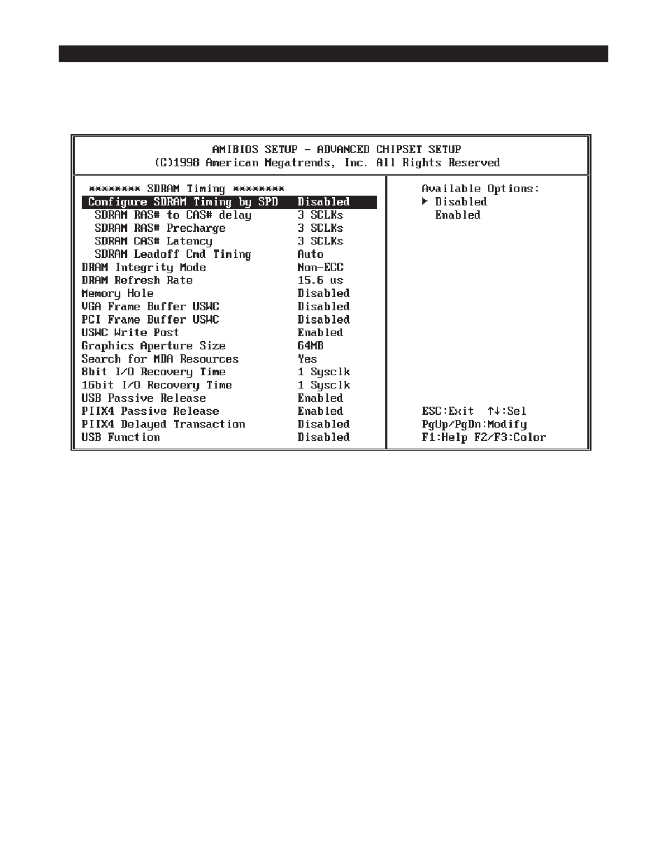
ADVANCED CHIPSET SETUP
These setup functions are working mostly for Chipset (Intel 440BX). These op-
tions are used to change the Chipset's registers. Carefully change any default set-
ting, otherwise the system will run unstably.
Configure SDRAM Timing by SPD >:
Enabled will select predetermined optimal values of chipset
parameters. When
Disabled
, chipset parameters return to setup information stored in CMOS.
SDRAM RAS# to CAS Delay >:
Used to specify the relative delay between row and column ad-
dress strobe from SDRAM.
SDRAM RAS# Precharge >:
This option specifies the length of time for Row Address Strobe
from SDRAM to precharge.
SDRAM CAS# Latency >:
Used to specify the CAS latency timing from SDRAM DRAM.
DRAM Integrity Mode >:
Used to choose DRAM Integrity Mode; ECC/EC will enable the Error
Checking and Correction DRAM integrity mode.
DRAM Refresh Rate >:
Used to specify the timing for DRAM Refresh.
Memory Hole >:
Used to specify the location of a memory hole in the CMOS RAM. This set-
ting reserves 15 to 16 MB memory address space for ISA expansion cards that specifi-
cally require this setting. Memory from 15 MB and up will be unavailable to the system
because expansion cards can only access memory up to 16 MB.
VGA Frame Buffer USWC >:
Used to specify whether or not a caching of the video A000-BFFF
RAM is allowed.
Enabled
will provide better system performance.
AMI BIOS Setup Menus
30
