Fifo buffers for transmitter and receiver – Intel 537EX User Manual
Page 93
536EX Chipset Developer’s Manual
93
Intel Confidential
Parallel Host Interface 16C450/16C550A UART
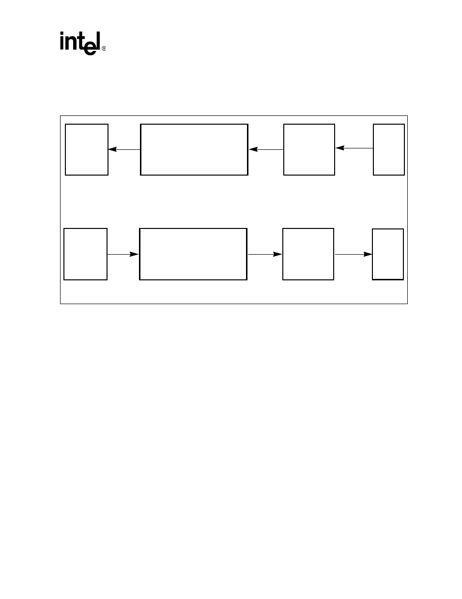
modem for each data interrupt, instead of only a single byte, as in 16C450 mode. The following
diagram shows how the FIFO is used. Host software using this FIFO capability can significantly
reduce system overhead by reducing the number of times that interrupt service routines are called.
The register addresses are divided into two types: single-register access and multiple-register
access. Most of the UART registers are single-register access (that is, only one internal register is
accessible for a given register address). UART register addresses 3–7 are used to access a single
internal register. The remainder of the UART register addresses (0–2) are used to access two or
more internal registers.
Register address 2 is used to write FIFO control information into the FCR (FIFO Control register)
and to read the IIR (Interrupt Identity register).
Register address 1 is used to read and write data to the IER (Interrupt Enable register) [when
DLAB = 0] and the MS DLM (Divisor Latch register) [when DLAB = 1].
Register address 0 is used to read data from the RBR (Receiver Buffer register) [when DLAB = 0],
write data to the THR (Transmitter Holding register) [when DLAB = 0], and read and write to the
LS DLL (Divisor Latch register) [when DLAB = 1]. The UART registers and FIFO usage are
described in the following sections.
Figure 12. FIFO Buffers for Transmitter and Receiver
Modem Transmitter FIFO
Transmitter
Transmitter
(THR)
Register
Holding
Shift
Register
UART Transmitter Flow Diagram
Modem Receiver FIFO
Receiver
Receiver
(RBR)
Register
Buffer
Shift
Register
UART Receiver Flow Diagram
UART
UART
Modem
Modem
Host
(DTE)
Host
(DTE)