Advanced chipset features – MSI MS-6566 User Manual
Page 53
Chapter 3
3-12
Advanced Chipset Features
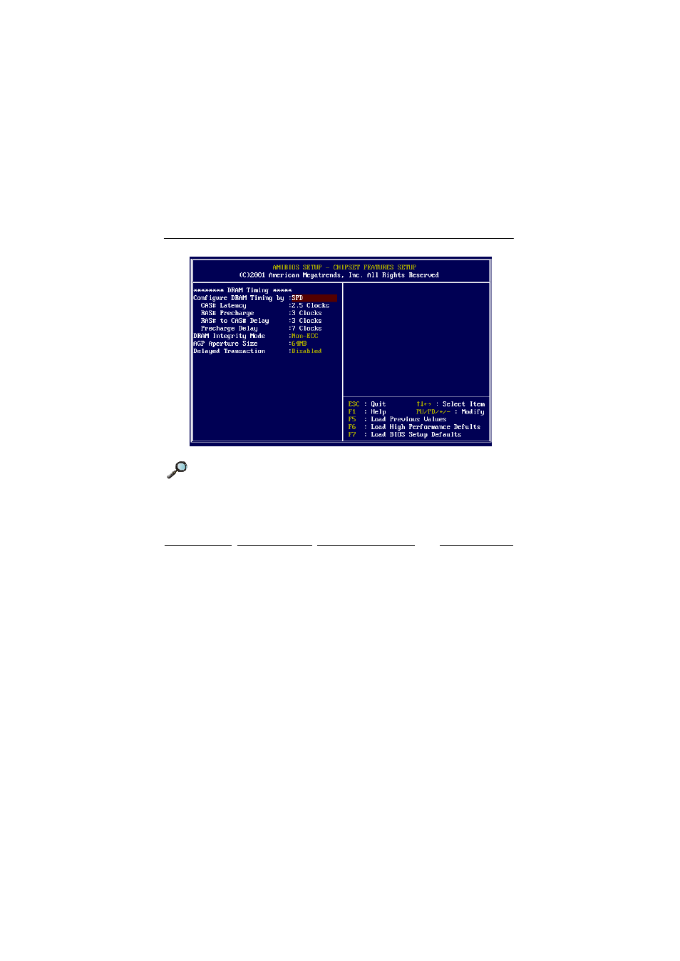
Configure DRAM Timing by
This setting determines whether DRAM timing is controlled by the SPD (Serial
Prese nce Detec t) EEPROM on the DR AM module . Setting to SPD enab les
CAS# Latency, RAS# Precharge, RAS# to CAS# Delay, and Precharge Delay
automatically to be determined by BIOS based on the configurations on the
SPD. Selecting Manual allows users to configure these fields manually.
CAS# Latency
The field controls the CAS latency, which determines the timing delay before
SDRAM starts a read command after receiving it. Setting options: 2.5 Clocks,
2 Clocks. 2 Clocks increases system p erformance while 2.5 Clocks prov ides
more stable system performance.
RAS# Precharge
This setting contro ls the number of cycles for Row Address Strobe (RAS) to
be allowed to precharge. If insufficient time is allowed for the RAS to accumu-
late its charge be fore DRAM refresh, refresh may be i ncomplete and DRAM
may fail to retain data. Th is item applies on ly when synchronou s DRAM is
Note: Change these settings only if you are familiar with the chipset.