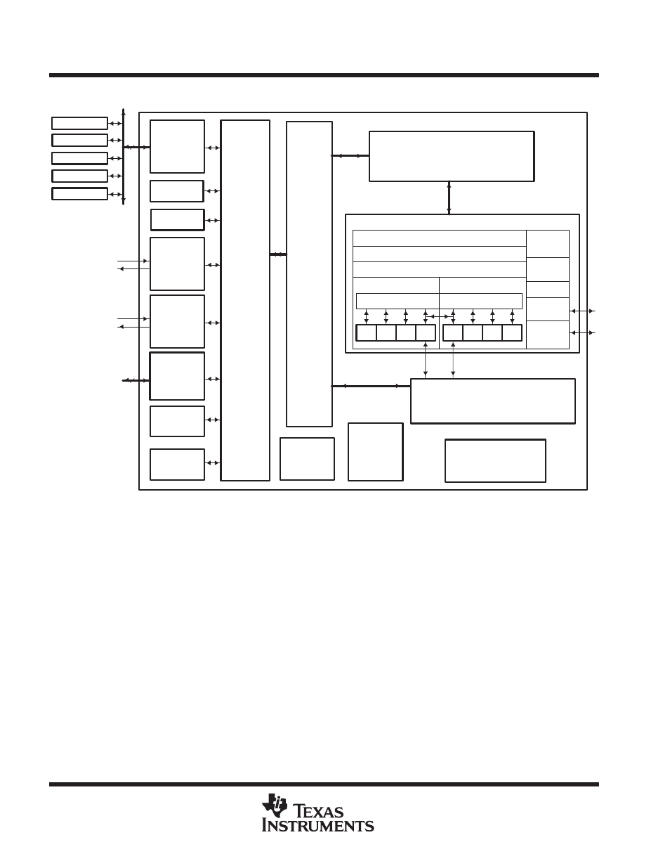
Functional block and cpu (dsp core) diagram – Motorola TMS320C6711D User Manual
Page 8

TMS320C6711D
FLOATINGĆPOINT DIGITAL SIGNAL PROCESSOR
SPRS292A − OCTOBER 2005 − REVISED NOVEMBER 2005
8
POST OFFICE BOX 1443
•
HOUSTON, TEXAS 77251−1443
functional block and CPU (DSP core) diagram
БББ
БББ
БББ
БББ
БББ
БББ
БББ
БББ
БББ
БББ
БББ
БББ
БББ
БББ
БББ
БББ
БББ
БББ
БББ
Test
C6000
CPU (DSP Core)
Data Path B
B Register File
Instruction Fetch
Instruction Dispatch
Instruction Decode
Data Path A
A Register File
Power-Down
Logic
.L1† .S1† .M1† .D1
.D2 .M2† .S2† .L2†
32
SDRAM
ROM/FLASH
SBSRAM
I/O Devices
L1P Cache
Direct Mapped
4K Bytes Total
Control
Registers
Control
Logic
L1D Cache
2-Way Set
Associative
4K Bytes Total
In-Circuit
Emulation
Interrupt
Control
Framing Chips:
H.100, MVIP,
SCSA, T1, E1
AC97 Devices,
SPI Devices,
Codecs
Digital Signal Processor
† In addition to fixed-point instructions, these functional units execute floating-point instructions.
‡ The device has a software-configurable PLL (with x4 through x25 multiplier and /1 through /32 divider).
Enhanced
DMA
Controller
(16 channel)
16
L2
Memory
4 Banks
64K Bytes
Total
PLL‡
Timer 0
External
Memory
Interface
(EMIF)
Multichannel
Buffered
Serial Port 1
(McBSP1)
Multichannel
Buffered
Serial Port 0
(McBSP0)
Host Port
Interface
(HPI)
SRAM
Timer 1
Boot
Configuration
Interrupt
Selector
GPIO
