Cache configuration (ccfg) register description, Cache configuration, Cache configuration register (ccfg) – Motorola TMS320C6711D User Manual
Page 42
TMS320C6711D
FLOATINGĆPOINT DIGITAL SIGNAL PROCESSOR
SPRS292A − OCTOBER 2005 − REVISED NOVEMBER 2005
42
POST OFFICE BOX 1443
•
HOUSTON, TEXAS 77251−1443
cache configuration (CCFG) register description
The device includes an enhancement to the
cache configuration (
CCFG) register. A “P” bit (CCFG.31) allows
the programmer to select the priority of accesses to L2 memory originating from the transfer crossbar (TC) over
accesses originating from the L1D memory system. An important class of TC accesses is EDMA transfers,
which move data to or from the L2 memory. While the EDMA normally has no issue accessing L2 memory due
to the high hit rates on the L1D memory system, there are pathological cases where certain CPU behavior could
block the EDMA from accessing the L2 memory for long enough to cause a missed deadline when transferring
data to a peripheral such as the McASP or McBSP. This can be avoided by setting the P bit to “1” because the
EDMA will assume a higher priority than the L1D memory system when accessing L2 memory.
For more detailed information on the P-bit function and for silicon advisories concerning EDMA L2 memory
accesses blocked, see the TMS320C6711/TMS320C6711B/TMS320C6711C/TMS320C6711D Digital Signal
Processors Silicon Errata (literature number SPRZ173K or later).
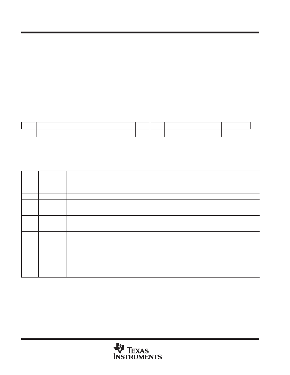
31
30
10
9
8
7
3
2
0
P
Reserved
IP
ID
Reserved
L2MODE
R/W-0
R-x
W-0
W-0
R-0 0000
R/W-000
Legend:
R = Readable; R/W = Readable/Writeable; -n = value after reset; -x = undefined value after reset
Figure 7.
Cache Configuration Register (CCFG)
Table 19. CCFG Register Bit Field Description
BIT #
NAME
DESCRIPTION
31
P
L1D requestor priority to L2 bit.
P = 0: L1D requests to L2 higher priority than TC requests
P = 1: TC requests to L2 higher priority than L1D requests
30:10
Reserved
Reserved. Read-only, writes have no effect.
9
IP
Invalidate L1P bit.
0
= Normal L1P operation
1
= All L1P lines are invalidated
8
ID
Invalidate L1D bit.
0
= Normal L1D operation
1
= All L1D lines are invalidated
7:3
Reserved
Reserved. Read-only, writes have no effect.
2:0
L2MODE
L2 operation mode bits (L2MODE).
000b = L2 Cache disabled (All SRAM mode) [64K SRAM]
001b = 1-way Cache (16K L2 Cache) / [48K SRAM]
010b = 2-way Cache (32K L2 Cache) / [32K SRAM]
011b = 3-way Cache (48K L2 Cache) / [16K SRAM]
111b = 4-way Cache (64K L2 Cache) / [no SRAM]
All others Reserved