General-purpose input/output (gpio) port timing, See figure 53) – Motorola TMS320C6711D User Manual
Page 101

TMS320C6711D
FLOATINGĆPOINT DIGITAL SIGNAL PROCESSOR
SPRS292 − OCTOBER 2005
101
POST OFFICE BOX 1443
•
HOUSTON, TEXAS 77251−1443
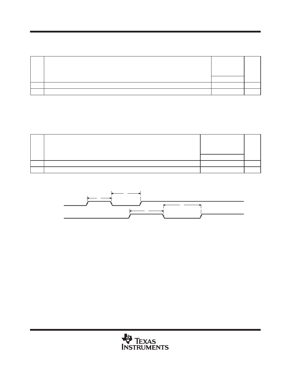
GENERAL-PURPOSE INPUT/OUTPUT (GPIO) PORT TIMING
timing requirements for GPIO inputs
†‡
(see Figure 53)
NO.
GDPA−167
ZDPA−167
−200
−250
UNIT
MIN
MAX
1
tw(GPIH)
Pulse duration, GPIx high
4P
ns
2
tw(GPIL)
Pulse duration, GPIx low
4P
ns
† P = 1/CPU clock frequency in ns. For example, when running parts at 250 MHz, use P = 4 ns.
‡ The pulse width given is sufficient to generate a CPU interrupt or an EDMA event. However, if a user wants to have the DSP recognize the GPIx
changes through software polling of the GPIO register, the GPIx duration must be extended to at least 24P to allow the DSP enough time to access
the GPIO register through the CFGBUS.
switching characteristics over recommended operating conditions for GPIO outputs
†§
(see Figure 53)
NO.
PARAMETER
GDPA−167
ZDPA−167
−200
−250
UNIT
MIN
MAX
3
tw(GPOH)
Pulse duration, GPOx high
12P − 3
ns
4
tw(GPOL)
Pulse duration, GPOx low
12P − 3
ns
† P = 1/CPU clock frequency in ns. For example, when running parts at 250 MHz, use P = 4 ns.
§ The number of CFGBUS cycles between two back-to-back CFGBUS writes to the GPIO register is 12 SYSCLK1 cycles; therefore, the minimum
GPOx pulse width is 12P.
GPIx
GPOx
4
3
2
1
Figure 53. GPIO Port Timing
