Motorola TMS320C6711D User Manual
Page 26
TMS320C6711D
FLOATINGĆPOINT DIGITAL SIGNAL PROCESSOR
SPRS292A − OCTOBER 2005 − REVISED NOVEMBER 2005
26
POST OFFICE BOX 1443
•
HOUSTON, TEXAS 77251−1443
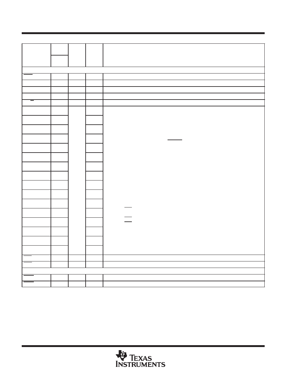
Terminal Functions (Continued)
SIGNAL
PIN
NO.
TYPE†
IPD/
‡
DESCRIPTION
SIGNAL
NAME
GDP/
ZDP
TYPE†
IPD/
IPU‡
DESCRIPTION
HOST-PORT INTERFACE (HPI)
HINT
J20
O
IPU
Host interrupt (from DSP to host)
HCNTL1
G19
I
IPU
Host control − selects between control, address, or data registers
HCNTL0
G18
I
IPU
Host control − selects between control, address, or data registers
HHWIL
H20
I
IPU
Host half-word select − first or second half-word (not necessarily high or low order)
HR/W
G20
I
IPU
Host read or write select
HD15
B14
IPU
Host-port data
•
Used for transfer of data, address, and control
HD14§
C14
IPU
•
Used for transfer of data, address, and control
•
Also controls initialization of DSP modes at reset via pullup/pulldown resistors
− Device Endian mode (HD8)
HD13§
A15
IPU
− Device Endian mode (HD8)
0
–
Big Endian
1
−
Little Endian
HD12§
C15
IPU
1
−
Little Endian
EMIF Big Endian mode correctness (EMIFBE) (HD12)
HD11
A16
IPU
EMIF Big Endian mode correctness (EMIFBE) (HD12)
0
–
The EMIF data will always be presented on the ED[7:0] side of the bus,
regardless of the endianess mode (Little/Big Endian).
HD10
B16
IPU
regardless of the endianess mode (Little/Big Endian).
1
−
In Little Endian mode (HD8 =1), the 8-bit or 16-bit EMIF data will be
present on the ED[7:0] side of the bus.
HD9
C16
IPU
present on the ED[7:0] side of the bus.
In Big Endian mode (HD8 =0), the 8-bit or 16-bit EMIF data will be present
on the ED[31:24] side of the bus [default].
HD8§
B17
I/O/Z
IPU
on the ED[31:24] side of the bus [default].
This new functionality does not affect systems using the curent default value of HD12=1. For
HD7
A18
I/O/Z
IPU
This new functionality does not affect systems using the curent default value of HD12=1. For
more detailed information on the big endian mode correctness, see the EMIF Big Endian Mode
Correctness portion of this data sheet.
HD6
C17
IPU
Correctness portion of this data sheet.
− Bootmode (HD[4:3])
HD5
B18
IPU
− Bootmode (HD[4:3])
00 –
HPI boot/Emulation boot
01 −
CE1 width 8-bit, Asynchronous external ROM boot with default timings
HD4§
C19
IPD
00 –
HPI boot/Emulation boot
01 −
CE1 width 8-bit, Asynchronous external ROM boot with default timings
(default mode)
10 −
CE1 width 16-bit, Asynchronous external ROM boot with default timings
HD3§
C20
IPU
(default mode)
10 −
CE1 width 16-bit, Asynchronous external ROM boot with default timings
11 −
CE1 width 32-bit, Asynchronous external ROM boot with default timings
HD2
D18
IPU
11 −
CE1 width 32-bit, Asynchronous external ROM boot with default timings
Other HD pins (HD [15:13, 11:9, 7:5, 2:0]) have pullups/pulldowns (IPUs/IPDs). For proper de-
HD1
D20
IPU
Other HD pins (HD [15:13, 11:9, 7:5, 2:0]) have pullups/pulldowns (IPUs/IPDs). For proper de-
vice operation of the HD[14, 13, 11:9, 7, 1, 0], do not oppose these pins with external IPUs/IPDs
at reset; however, the HD[15, 6, 5, 2] pins can be opposed and driven during reset.
HD0
E20
IPU
at reset; however, the HD[15, 6, 5, 2] pins can be opposed and driven during reset.
For more details, see the Device Configurations section of this data sheet.
HAS
E18
I
IPU
Host address strobe
HCS
F20
I
IPU
Host chip select
EMIF − CONTROL SIGNALS COMMON TO ALL TYPES OF MEMORY¶
HDS1
E19
I
IPU
Host data strobe 1
HDS2
F18
I
IPU
Host data strobe 2
† I = Input, O = Output, Z = High impedance, S = Supply voltage, GND = Ground, A = Analog signal (PLL Filter)
‡ IPD = Internal pulldown, IPU = Internal pullup. [To oppose the supply rail on these IPD/IPU signal pins, use external pullup or pulldown resistors
no greater than 4.4 k
Ω
and 2.0 k
Ω
, respectively.]
§ To ensure a proper logic level during reset when these pins are both routed out and 3−stated or not driven, it is recommended an external 10-k
Ω
pullup/pulldown resistor be included to sustain the IPU/IPD, respectively.
¶ To maintain signal integrity for the EMIF signals, serial termination resistors should be inserted into all EMIF output signal lines.