Motorola TMS320C6711D User Manual
Page 29
TMS320C6711D
FLOATINGĆPOINT DIGITAL SIGNAL PROCESSOR
SPRS292A − OCTOBER 2005 − REVISED NOVEMBER 2005
29
POST OFFICE BOX 1443
•
HOUSTON, TEXAS 77251−1443
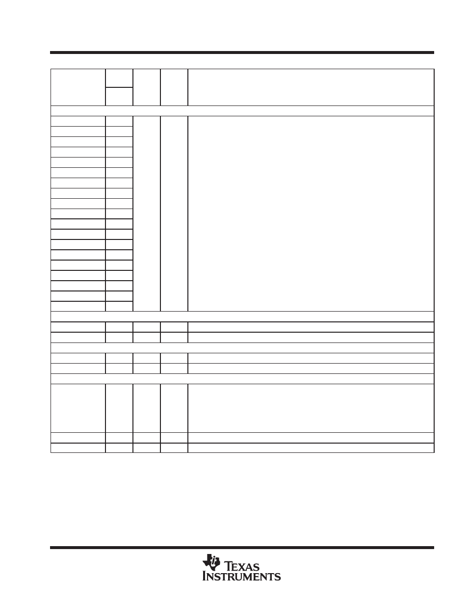
Terminal Functions (Continued)
SIGNAL
PIN
NO.
TYPE†
IPD/
‡
DESCRIPTION
SIGNAL
NAME
GDP/
ZDP
TYPE†
IPD/
IPU‡
DESCRIPTION
EMIF − DATA (CONTINUED)¶
ED18
Y3
ED17
W4
ED16
V4
ED15
T19
ED14
T20
ED13
T18
ED12
R20
ED11
R19
ED10
P20
ED9
P18
I/O/Z
IPU
External data
ED8
N20
I/O/Z
IPU
External data
ED7
N19
ED6
N18
ED5
M20
ED4
M19
ED3
L19
ED2
L18
ED1
K19
ED0
K18
TIMER 1
TOUT1
F1
O
IPD
Timer 1 or general-purpose output
TINP1
F2
I
IPD
Timer 1 or general-purpose input
TIMER 0
TOUT0
G1
O
IPD
Timer 0 or general-purpose output
TINP0
G2
I
IPD
Timer 0 or general-purpose input
MULTICHANNEL BUFFERED SERIAL PORT 1 (McBSP1)
CLKS1
E1
I
IPD
External clock source (as opposed to internal)
On the device, this pin does not have an internal pulldown (IPD). For proper device opera-
tion, the CLKS1 pin should either be driven externally at all times or be pulled up with a 10-k
Ω
resistor to a valid logic level. Because it is common for some ICs to 3-state their outputs at
times, a 10-k
Ω
pullup resistor may be desirable even when an external device is driving the
pin.
CLKR1
M1
I/O/Z
IPD
Receive clock
CLKX1
L3
I/O/Z
IPD
Transmit clock
† I = Input, O = Output, Z = High impedance, S = Supply voltage, GND = Ground, A = Analog signal (PLL Filter)
‡ IPD = Internal pulldown, IPU = Internal pullup. [To oppose the supply rail on these IPD/IPU signal pins, use external pullup or pulldown resistors
no greater than 4.4 k
Ω
and 2.0 k
Ω
, respectively.]
¶ To maintain signal integrity for the EMIF signals, serial termination resistors should be inserted into all EMIF output signal lines.