Synchronous dram timing, See figure 31), See figure 31−figure 37) – Motorola TMS320C6711D User Manual
Page 76
TMS320C6711D
FLOATINGĆPOINT DIGITAL SIGNAL PROCESSOR
SPRS292A − OCTOBER 2005 − REVISED NOVEMBER 2005
76
POST OFFICE BOX 1443
•
HOUSTON, TEXAS 77251−1443
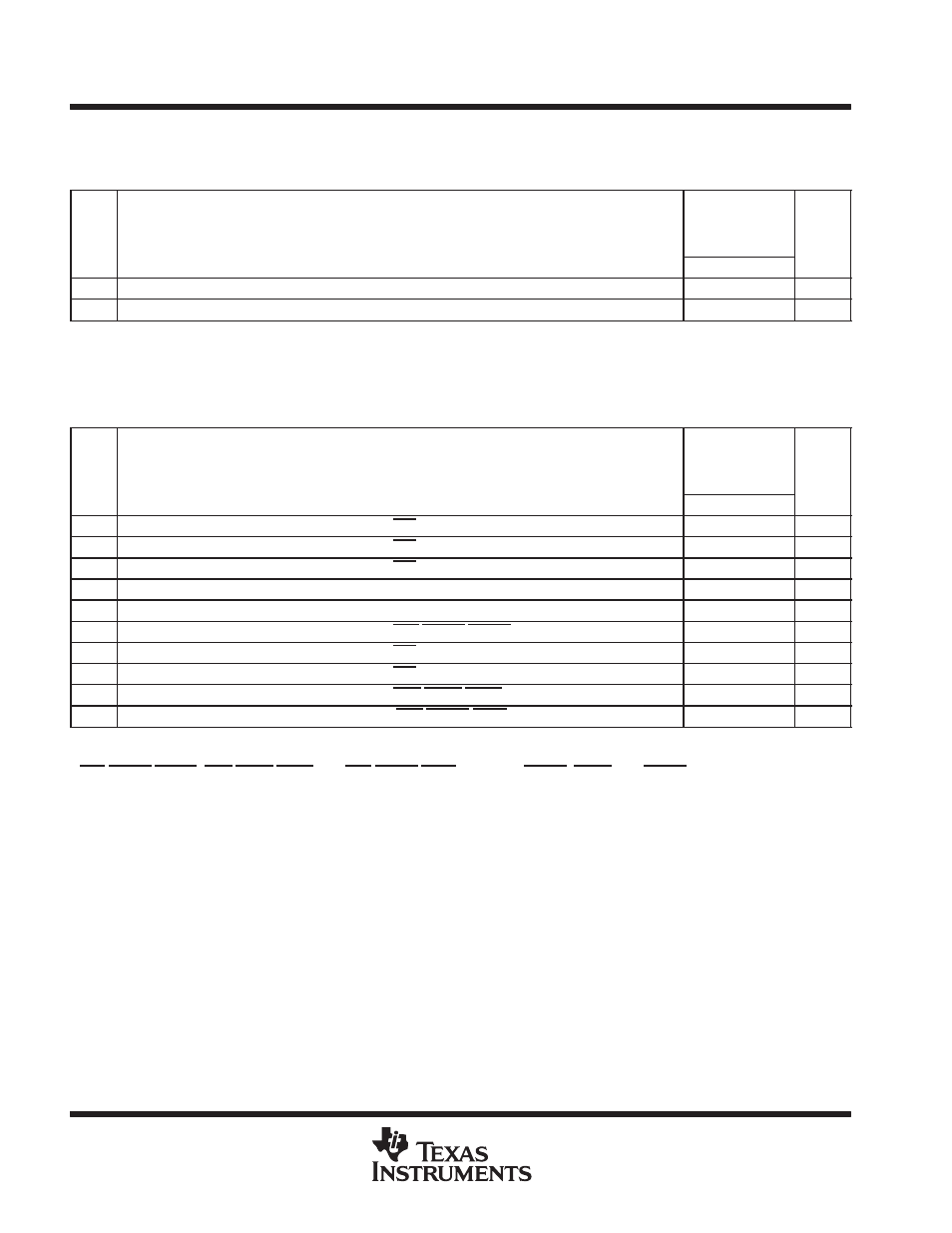
SYNCHRONOUS DRAM TIMING
timing requirements for synchronous DRAM cycles
†
(see Figure 31)
NO.
GDPA-167
ZDPA−167
−200
−250
UNIT
MIN
MAX
6
tsu(EDV-EKOH)
Setup time, read EDx valid before ECLKOUT high
1.5
ns
7
th(EKOH-EDV)
Hold time, read EDx valid after ECLKOUT high
2.5
ns
† The SDRAM interface takes advantage of the internal burst counter in the SDRAM. Accesses default to incrementing 4-word bursts, but random
bursts and decrementing bursts are done by interrupting bursts in progress. All burst types can sustain continuous data flow.
switching characteristics over recommended operating conditions for synchronous DRAM
cycles
†‡
(see Figure 31−Figure 37)
NO.
PARAMETER
GDPA-167
ZDPA−167
−200
−250
UNIT
MIN
MAX
1
td(EKOH-CEV)
Delay time, ECLKOUT high to CEx valid
1.5
7
ns
2
td(EKOH-BEV)
Delay time, ECLKOUT high to BEx valid
7
ns
3
td(EKOH-BEIV)
Delay time, ECLKOUT high to BEx invalid
1.5
ns
4
td(EKOH-EAV)
Delay time, ECLKOUT high to EAx valid
7
ns
5
td(EKOH-EAIV)
Delay time, ECLKOUT high to EAx invalid
1.5
ns
8
td(EKOH-CASV) Delay time, ECLKOUT high to ARE/SDCAS/SSADS valid
1.5
7
ns
9
td(EKOH-EDV)
Delay time, ECLKOUT high to EDx valid
7
ns
10
td(EKOH-EDIV)
Delay time, ECLKOUT high to EDx invalid
1.5
ns
11
td(EKOH-WEV)
Delay time, ECLKOUT high to AWE/SDWE/SSWE valid
1.5
7
ns
12
td(EKOH-RAS)
Delay time, ECLKOUT high to, AOE/SDRAS/SSOE valid
1.5
7
ns
† The SDRAM interface takes advantage of the internal burst counter in the SDRAM. Accesses default to incrementing 4-word bursts, but random
bursts and decrementing bursts are done by interrupting bursts in progress. All burst types can sustain continuous data flow.
‡ ARE/SDCAS/SSADS, AWE/SDWE/SSWE, and AOE/SDRAS/SSOE operate as SDCAS, SDWE, and SDRAS, respectively, during SDRAM
accesses.