8 transmitting data, 8 .1 .8 transmitting data -6, Figure 8-5 . master i – Maxim Integrated MAX31782 User Manual
Page 74: C data flowchart -6, Figure 8-5, 8transmittingdata
MaximIntegrated 8-6
MAX31782 User’s Guide
Revision 0; 8/11
Upon transmitting the slave data byte (7 bits of slave address + R/W bit + acknowledge), the I
2
C master controller will
enter one of the three states .
• Data Transmit: The I2CMODE (R/W) bit was set to a 0, indicating that the master will be writing data to a slave device .
The MAX31782 will retain control of the SDA line .
• Data Receive: The I2CMODE (R/W) bit was set to a 1, indicating that the master will be receiving data from a slave .
The MAX31782 releases control of SDA to allow a slave device to output data . The MAX31782 master I
2
C controller
automatically begins clocking bytes of data from the slave .
• The slave address was NACKed . The master I
2
C controller will retain control of SDA and is able to transmit data .
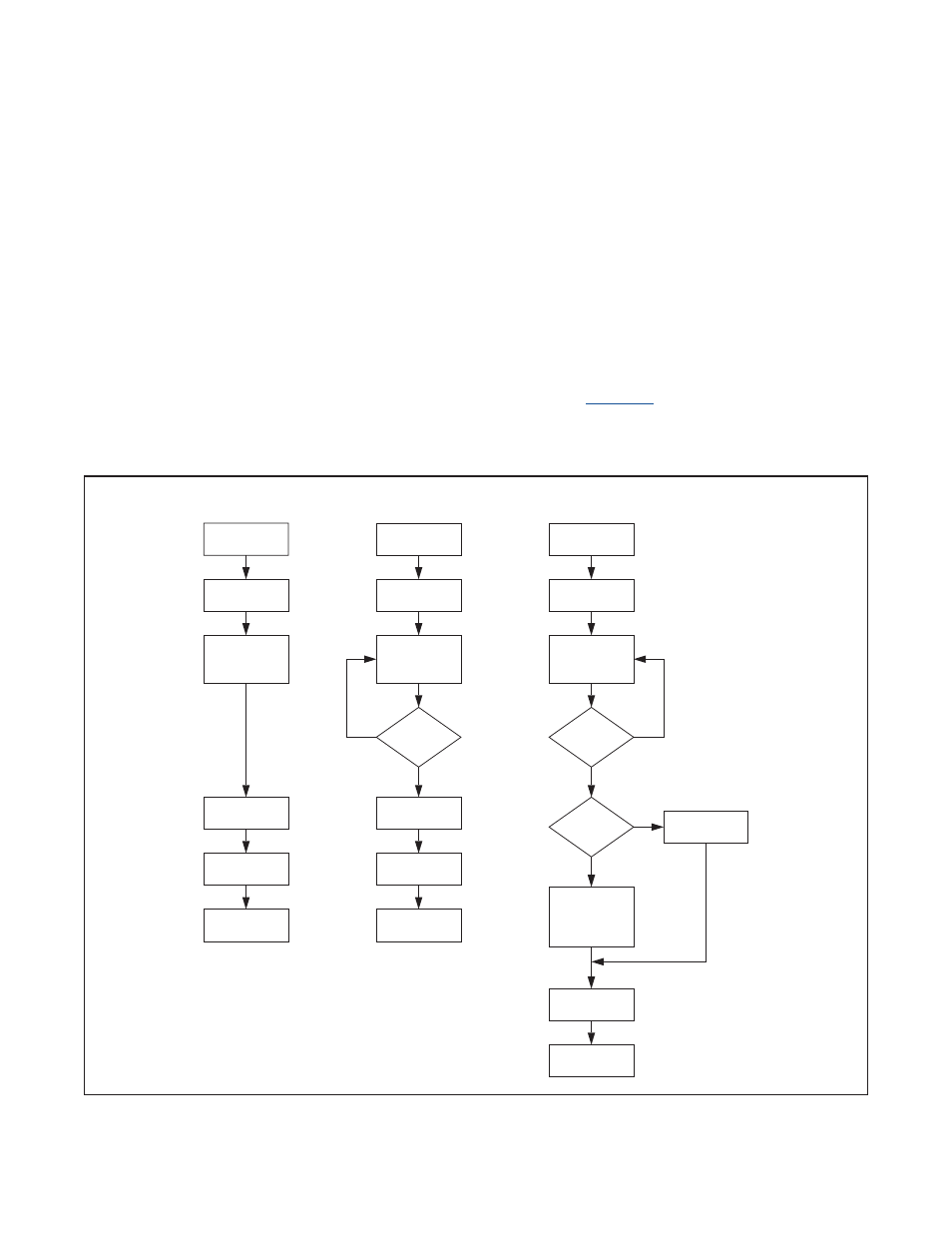
8.1.8TransmittingData
The MAX31782 I
2
C master controller enters into data transmission mode after transmitting a slave address with the
R/W bit (I2CMODE) set to a 0 . The steps of data transmission are shown in
. Data transmission is started by
software loading a byte of data into the I2CBUF_M register . Loading I2CBUF_M causes the I2CBUSY bit to be set . Once
set, writes to I2CBUF_M will be ignored . The first bit of data (most significant bit) will be shifted to SDA when SCL is low .
Each of the next seven bits will then be shifted following high to low transitions of SCL .
Figure 8-5. Master I
2
C Data Flowchart
WRITE TO
I2CBUF_M
TRANSMITTING
SLAVE ADDRESS
I2CBUSY = 1
Y
N
N
8 BITS
TRANSMIT?
TRANSMIT
I2CBUF_M[6:0] +
I2CMODE
RECEIVE
ACKNOWLEDGE
I2CNACKI =
ACKNOWLEDGE
I2CTXI = 1
I2CBUSY = 0
I2CNACKI =
ACKNOWLEDGE
I2CTXI = 1
I2CBUSY = 0
I2CROI = 1
Y
WRITE TO
I2CBUF_M
TRANSMITTING
BYTE
I2CBUSY = 1
TRANSMIT SHIFT
REGISTER BYTE,
MSB FIRST
RECEIVE
ACKNOWLEDGE
Y
8 BITS
RECEIVED?
RECEIVER
FULL?
N
I2CBUSY = 1
SEND
I2CACK
I2CBUSY = 0
RECEIVE A BIT INTO
SHIFT REGISTER,
MSB FIRST
LOAD SHIFT
REGISTER INTO
I2CBUF_M
I2CRXI = 1
FIRST SCL RISING
EDGE GENERATED
RECEIVING
BYTE