6 smbus mode selection register (smbus), 7 i2c slave clock control register (i2cck_s), 8 i2c slave timeout register (i2cto_s) – Maxim Integrated MAX31782 User Manual
Page 68: C slave clock control register (i2cck_s) -12, 7 .2 .8 i, C slave timeout register (i2cto_s) -12, 6smbusmodeselectionregister(smbus), Cslaveclockcontrolregister(i2cck�s), Cslavetimeoutregister(i2cto�s), C slave interface (sda and scl) and the i
MaximIntegrated 7-12
MAX31782 User’s Guide
Revision 0; 8/11
7.2.6SMBusModeSelectionRegister(SMBUS)
Address: M3[04h]
This register contains bits that are used for both the I
2
C slave interface (SDA and SCL) and the I
2
C master interface
(MSDA and MSCL) . For operation of the slave interface, only the slave bits should be used .
7.2.7I
2
CSlaveClockControlRegister(I2CCK�S)
Address: M2[0Dh]
This register has no function when operating in slave mode .
7.2.8I
2
CSlaveTimeoutRegister(I2CTO�S)
Address: M2[0Eh]
This register has no function when operating in slave mode .
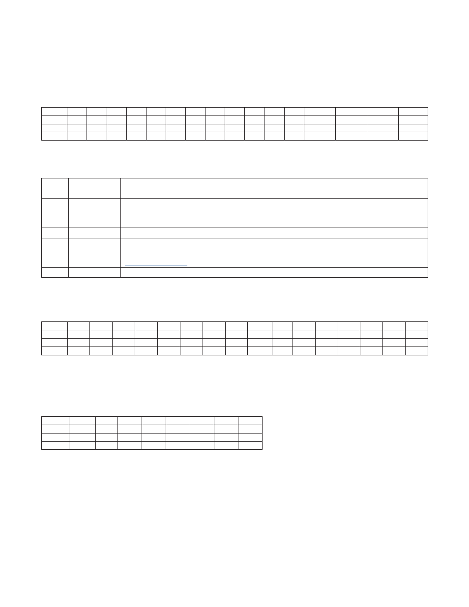
Bit
15
14
13
12
11
10
9
8
7
6
5
4
3
2
1
0
Name
—
—
—
—
—
—
—
—
—
—
—
—
RESET_S
RESET_M
SMB_MOD_S SMB_MOD_M
Reset
0
0
0
0
0
0
0
0
0
0
0
0
0
0
0
0
Access
r
r
r
r
r
r
r
r
r
r
r
r
rw
rw
rw
rw
BIT
NAME
DESCRIPTION
15:4
—
Reserved . The user should not write to these bits .
3
RESET_S
I
2
C Slave Reset Bit . This bit can be used by the software to unconditionally reset and disable the I
2
C
slave interface . After at least one system clock cycle, this bit must be cleared by software . After this
bit is toggled, all the relevant I
2
C slave registers need to be reinitialized .
2
RESET_M
This bit does not affect the slave I
2
C interface (SDA and SCL) .
1
SMB_MOD_S
Slave SMBus Mode Operation . When this bit is set to a 1, SMBus timeout functionality is enabled for
the I
2
C slave interface . When this bit is cleared to 0, the SMBus timeout functionality is disabled . See
0
SMB_MOD_M
This bit does not affect the slave I
2
C interface (SDA and SCL) .
Bit
15
14
13
12
11
10
9
8
7
6
5
4
3
2
1
0
Name
I2CCKH7 I2CCKH6 I2CCKH5 I2CCKH4 I2CCKH3 I2CCKH2 I2CCKH1 I2CCKH0 I2CCKL7 I2CCKL6 I2CCKL5 I2CCKL4 I2CCKL3 I2CCKL2 I2CCKL1 I2CCKL0
Reset
0
0
0
1
0
0
1
1
0
0
0
1
0
0
1
1
Access
rw
rw
rw
rw
rw
rw
rw
rw
rw
rw
rw
rw
rw
rw
rw
rw
Bit
7
6
5
4
3
2
1
0
Name
I2CTO7
I2CTO6
I2CTO5
I2CTO4
I2CTO3
I2CTO2
I2CTO1
I2CTO0
Reset
0
0
0
0
0
0
0
0
Access
rw
rw
rw
rw
rw
rw
rw
rw