Transmit side functions, Transmit side functions -5, Data receiver -5 serial fifo buffer -5 – Verilink DIU 2130 (880-503297-001) Product Manual User Manual
Page 15: Data receiver, Serial fifo buffer
DIU 2130 Overview
Verilink
1-5
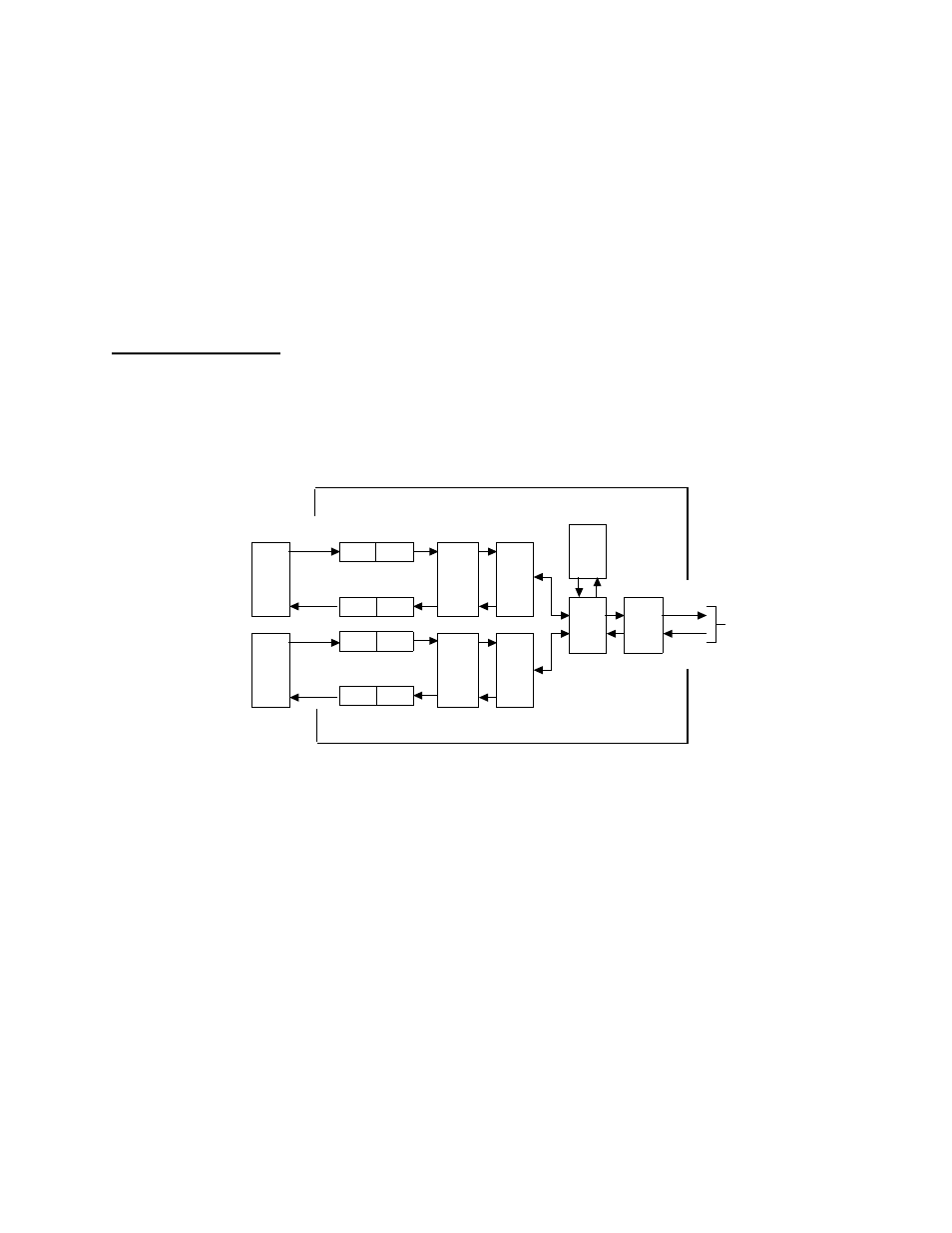
Figure 1-7 shows the signals conveyed between the DIUs and
associated CSU on the assigned data bus. In the transmit direction
toward the network, the data bus sends the output data from each
DIU to the CSU of the NCC or TAC. It also sends clocking and
framing information from the CSU to the DIUs. The transmit clock
synchronizes the DIU transmit side circuits to the CSU.
In the incoming direction from the network, the data bus sends the
data from the CSU to the DIU. It also furnishes receive clocking and
framing information to the DIU for synchronization of the DIU’s
receiver to the CSU.
Transmit Side
Functions
The DIU transmit data port accepts the data from the customer
equipment for the designated DS0 channels. The data from both
ports is multiplexed and sent to the associated CSU through the
assigned data bus.
Figure 1-8 DIU 2130 Block Diagram
Data Receiver
The data receiver converts the V.35, RS-449, or EIA 530 data and
control signals to a format suitable for internal DIU processing.
The data signals are in a balanced differential format. The control
and timing signals are either balanced or unbalanced, depending
on the interface used.
Serial FIFO Buffer
Each DIU input/output (I/O) port is equipped with a 256
×
1 bit
first-in, first-out (FIFO) buffer at the data interface. The FIFO
provides elastic buffering between the data equipment and the DIU
to accommodate short-term timing differences between them
without loss of data.
DATA
EQ 1
DATA
EQ 2
INTF
LOGIC,
LPBK
MUX &
SCRAM-
BLER
CLOCK
GEN &
FIFO
CLOCK
GEN &
FIFO
MUX/
DEMUX
TEST
CODE
GEN/
DET
DRVRS
&
RCVRS
DATA
OUT
DATA
IN
TO/FROM
BACKPLANE
DATA BUS
XMT DATA
& CLOCK
XMT DATA
& CLOCK
RCV DATA
& CLOCK
RCV DATA
& CLOCK
DIU 2130
FIFO
FIFO
FIFO
FIFO
DRVR
DRVR
RCVR
RCVR
INTF
LOGIC,
LPBK
MUX &
SCRAM-
BLER