2 functional description, 1 block diagram, 2 module description – Sundance SMT941 User Manual
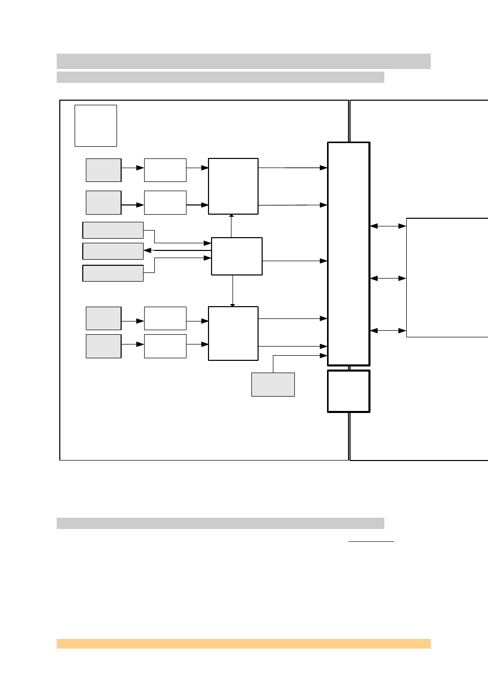
Page 8: Figure 1 - smt942 block diagram
User Manual SMT941
Last Edited: 23/08/2011 17:24:00
2 Functional Description
2.1 Block Diagram
SLB Base Module (In this case SMT351T)
SMT941 (SLB Mezzanine Module)
Virtex-5
XC5VLX50T, SX50T, SX95T, LX110T
FF1136 Package
Channel A
Signal
Conditioning
(AC-coupling)
Channel B
Signal
Conditioning
(AC-coupling)
ADC Input
Ch A MMCX
50-Ohm
ADC Input
Ch B MMCX
50-Ohm
Daughter Card
interface
connector
SLB
RSLA
ADC ChannelA and
ChannelB
RSLB
DAC ChannelA and
ChannelB
Top and Bottom TIM
Connectors
ChA
– 1.8V DDR LVDS,
Clock and Control
Data and Clocks
4xComports (0,1,3 and 4)
ADS62P49
Dual ADC ChA&B
14-bit 250MSPS
(2x675mW)
Channel C
Signal
Conditioning
(AC-coupling)
Channel D
Signal
Conditioning
(AC-coupling)
ADC Output
Ch C MMCX
50-Ohm
ADC Output
Ch D MMCX
50-Ohm
ADS62P49
Dual ADC ChA&B
14-bit 250MSPS
(2x675mW)
Power
Daughter Card
connector
SLB
ChD
– 1.8V DDR LVDS,
Clock and Control
ChC
– 1.8V DDR LVDS,
Clock and Control
Bank A
2.5V
Bank B
2.5V
Bank C
2.5V
Power
Supplies: 1.8
and 3.3 Volts
(Linear
Regulators)
Power
Supplies: 1.0,
1.2, 1.8, 2.5
and 3.3 Volts
External Trigger
Clock Synchronizer
and Jitter Cleaner
based on
CDCE72010 (1.8W)
ADCs External Clock In
- MMCX
External Reference
Clock In - MMCX
FPGA Clock
ChB
– 1.8V DDR LVDS,
Clock and Control
ADCs External Clock
Out - MMCX
Data and Clocks
Figure 1 - SMT942 Block diagram.
2.2 Module Description
The SMT941 has got 2 dual channel Analog-to-Digital converters
– Texas
Instrument) that have been designed for multi-carrier, wide bandwidth
communication applications. All 4 analog inputs are available on MMCX connectors.
They are 50-Ohm AC-coupled inputs (RF transformers - ration 1). DDR LVDS lines
are used to carry samples through the SLB connector to the FPGA (SLB base module
– FPGA IOs must be 2.5-Volt).
A clock distribution chip ensures that all converters sample synchronously to a
single clock source. The clock source can be external or internal (on-board 245.76-