Adc chcd register 3 0x43, Adc chcd register 4 0x44 – Sundance SMT941 User Manual
Page 35
User Manual SMT941
Page 35 of 43
Last Edited: 23/08/2011 17:24:00
3
‘111’
Falling edge shifted by -(4/26)/Sampling Frequency
Setting
Bit 15:13
Description Clock output Edge control (rising edge)
0
‘000’,’100’ Default output clock position.
1
‘101’
Rising edge shifted by +(4/26)/Sampling Frequency
2
‘110’
Rising edge shifted by -(6/26)/Sampling Frequency
3
‘111’
Rising edge shifted by -(4/26)/Sampling Frequency
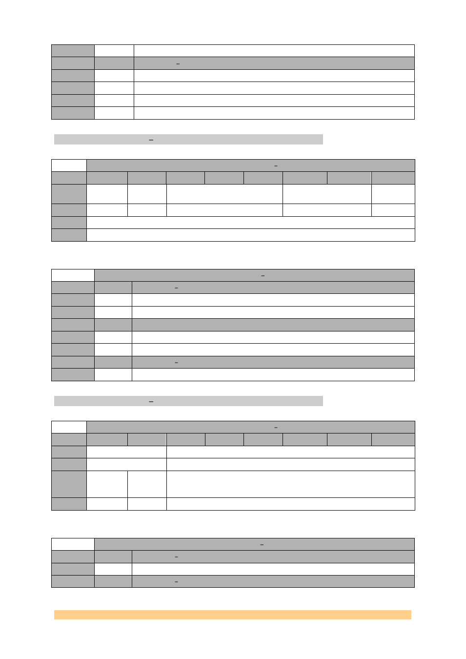
ADC Chcd Register 3 0x43.
ADC Chcd Register 3 0x43
Byte
Bit 7
Bit 6
Bit 5
Bit 4
Bit 3
Bit 2
Bit 1
Bit 0
0
Reserved
Channel
Control
Reserved
Data Format
Reserved
Default
’0’
‘0’
‘000’
‘00’
‘0’
1
Custom Pattern (lsb)
Default
‘00000000’
ADC Chcd Register 3 0x43
Setting
Bit 2:1
Description Data Format
0
‘10’
2’s complement.
1
‘11’
Binary.
Setting
Bit 6
Description - Channel Control
0
‘0’
Common Control.
1
‘1’
Independent Control (Test pattern, Offset correction and SNR boost).
Setting
Bit 15:8
Description Custom Pattern (lsb)
0
ADC Chcd Register 4 0x44.
ADC Chcd Register 4 0x44
Byte
Bit 7
Bit 6
Bit 5
Bit 4
Bit 3
Bit 2
Bit 1
Bit 0
0
Reserved
Custom Pattern (msb)
Default
‘00’
‘000000’
1
Reserved
Offset
Correctio
n Enable
Reserved
Default
‘0’
‘0’
‘000000’
ADC Chcd Register 4 0x44
Setting
Bit 5:0
Description Custom Pattern (msb).
0
Setting
Bit 14
Description Offset Correction Enable ChA.