2 reading and writing registers – Sundance SMT941 User Manual
Page 12
User Manual SMT941
Page 12 of 43
Last Edited: 23/08/2011 17:24:00
Byte
Bit 7
Bit 6
Bit 5
Bit 4
Bit 3
Bit 2
Bit 1
Bit 0
3
Command
3
Command
2
Command
1
Command
0
Address
11
Address
10
Address 9
Address 8
2
Address 7
Address 6
Address 5
Address 4
Address 3
Address 2
Address 1
Address 0
1
Data 15
Data 14
Data 13
Data 12
Data 11
Data 10
Data 9
Data 8
0
Data 7
Data 6
Data 5
Data 4
Data 3
Data 2
Data 1
Data 0
Figure 4
– Setup Packet Structure.
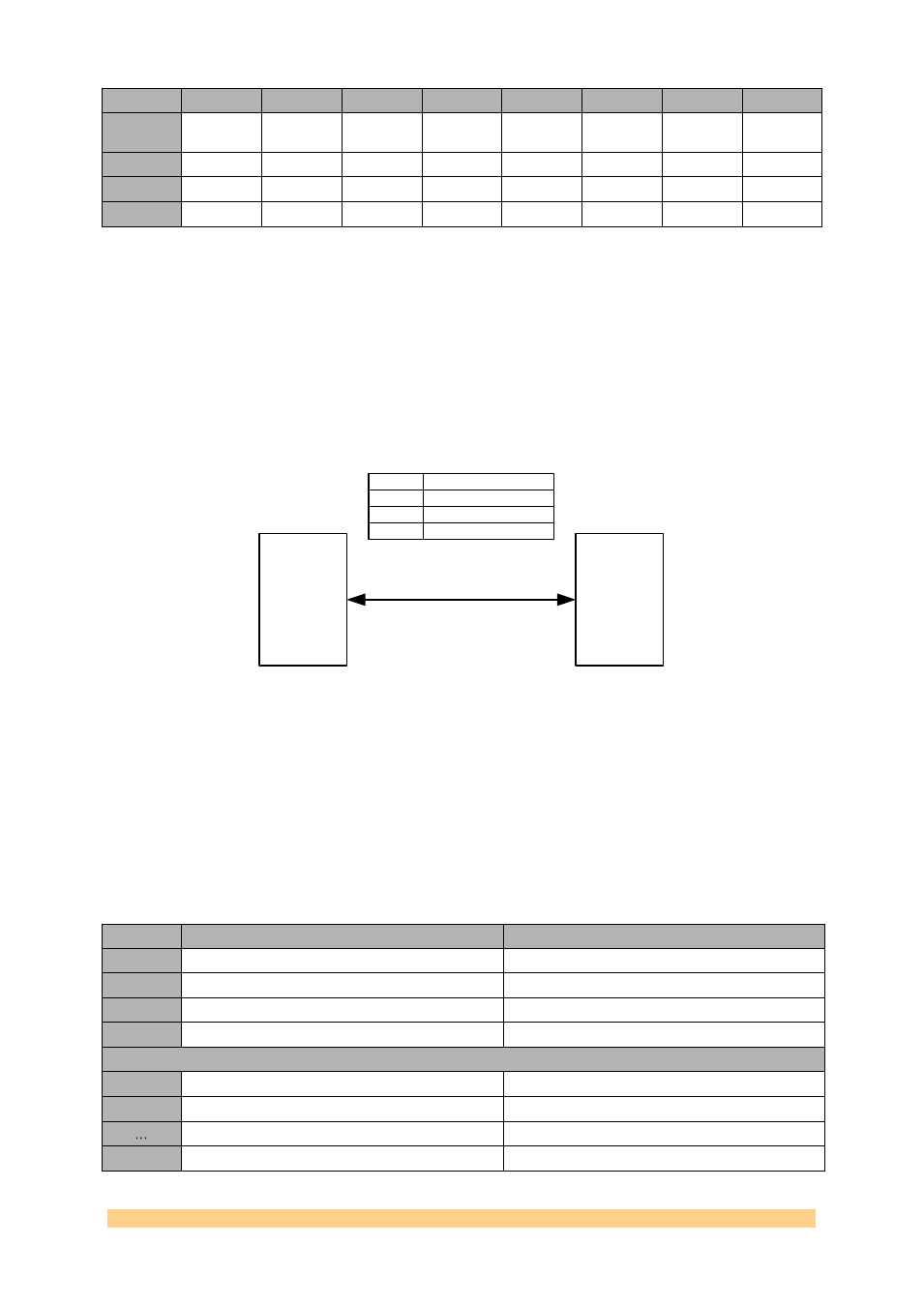
2.3.1.2 Reading and Writing Registers
Control packets are sent to the SMT941 over Comport3. This is a bi-directional
interface. The format of a ‘Read Packet’ is the same as that of a write packet.
Host
Fixed Sequence
SMT941
ComPort 3
Byte 0
Read/Write Address
Byte 1
Read/Write Data
Byte 3
Read/Write Data
Byte 4
1) Write Packet
Figure 5
– Control Register Read Sequence.
2.3.1.3 Memory Map
The write packets must contain the address where the data must be written to and
the read packets must contain the address where the required data must be read.
The following figure shows the memory map for the writable and readable Control
Registers on the SMT941:
Address
Writable Registers
Readable Registers
0x00
Reserved.
Reserved.
0x01
Board Control Register.
Firmware Version.
0x02
Reserved.
Clock Readback Register.
0x03
Reserved.
Board Status Register
Clock Section
0x10
Clock Register 0x0.
Read-back (FPGA Register) Clock Register 0x0.
0x11
Clock Register 0x1.
Read-back (FPGA Register) Clock Register 0x1.
…
…
0x28
Clock Register 0x18.
Read-back (FPGA Register) Clock Register 0x18.