Adc chab register 2 0x32, Adc chab register 3 0x33 – Sundance SMT941 User Manual
Page 28
User Manual SMT941
Page 28 of 43
Last Edited: 23/08/2011 17:24:00
1
‘1’
Both ADC channels are put into standby mode (internal ref and output buffers still
active).
Setting
Bit 6:5
Description Reference.
0
‘01’
Internal Reference enabled.
1
‘11’
External Reference enabled.
Setting
Bit 11:8
Description Power down modes.
0
‘0000’
Pins ctrl1, 2 and 3 determine power down modes.
1
‘1000’
Normal mode of operation.
2
‘1001’
Output buffers disabled for channelB.
3
‘1010’
Output buffers disabled for channelA.
4
‘1011’
Output buffers disabled for channelA and B.
5
‘1100’
Global power down.
6
‘1101’
ChannelB in standby.
7
‘1110’
ChannelA in standby.
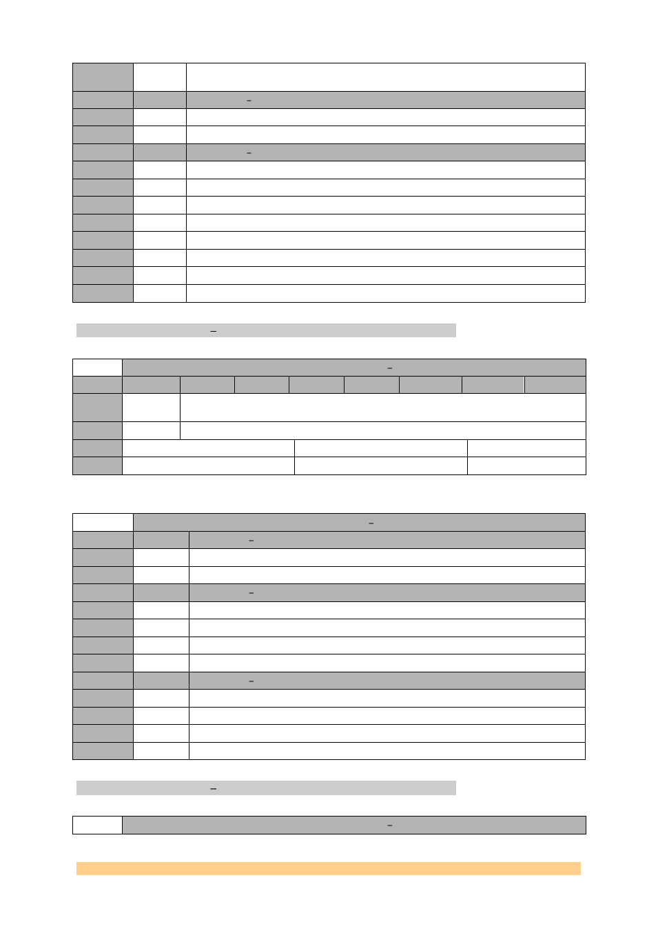
ADC Chab Register 2 0x32.
ADC Chab Register 2 0x32
Byte
Bit 7
Bit 6
Bit 5
Bit 4
Bit 3
Bit 2
Bit 1
Bit 0
0
LVDS_CM
OS
Reserved
Default
’0’
‘0000000’
1
Clock Edge Control (rising edge)
Clock Edge Control (falling edge)
Reserved
Default
‘000’
‘000’
‘00’
ADC Chab Register 2 0x32
Setting
Bit 7
Description LVDS_CMOS
0
‘0’
Parallel CMOS interface.
1
‘1’
DDR LVDS interface.
Setting
Bit 12:10
Description Clock output Edge control (falling edge)
0
‘000’,’100’ Default output clock position.
1
‘101’
Falling edge shifted by +(4/26)/Sampling Frequency
2
‘110’
Falling edge shifted by -(6/26)/Sampling Frequency
3
‘111’
Falling edge shifted by -(4/26)/Sampling Frequency
Setting
Bit 15:13
Description Clock output Edge control (rising edge)
0
‘000’,’100’ Default output clock position.
1
‘101’
Rising edge shifted by +(4/26)/Sampling Frequency
2
‘110’
Rising edge shifted by -(6/26)/Sampling Frequency
3
‘111’
Rising edge shifted by -(4/26)/Sampling Frequency
ADC Chab Register 3 0x33.
ADC Chab Register 3 0x33