Figure 2 - clock structure - block diagram, External reference input – Sundance SMT941 User Manual
Page 10
User Manual SMT941
Page 10 of 43
Last Edited: 23/08/2011 17:24:00
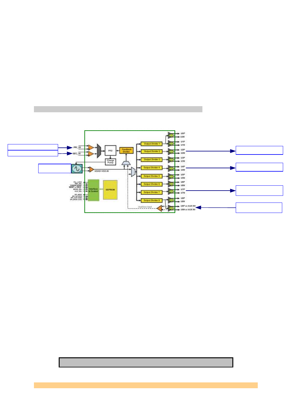
2.2.2 Clock structure
The following diagram shows the clock structure of the SMT941:
Clock Synthesizer and Jitter Cleaner - Texas Instrument CDCE72010
U2 - ADC Channel a&b
U7 - Clk Out and FPGA
Clk Output (ExtClkOut)
FPGA (SLB)
Clk In
Clk Input (ExtClkIn)
On-board VCXO
254.76 MHz
On-board 10-MHz reference
External Reference (ExtRefIn)
ADC Chc&d
– ADS62P49
14-bit 250MSPS
U4 - ADC Channel a&b
ADC Cha&b
– ADS62P49
14-bit 250MSPS
Figure 2 - Clock Structure - Block Diagram
The clock distribution chip used on the SMT941 offers 2 reference inputs, a VCXO
differential input and a charge pump to drive the VCXO, as well as a second
differential clock input. ADCs and external clock are mapped to separate internal
output dividers in order to give more flexibility.
The CDCE72010 chip is designed to provide clean, phase related clocks to the
converters. The reference clock (on-board or external) is used to lock the on-board
VCXO using the clock chip PLL/charge pump. It is also possible to feed an external
sampling clock to the chip that can then be distributed the analog converters.
Note that when the board is mounted onto a PXI SLB carrier such as the SMT700
(with 2.5-Volt FPGA IOs), it is possible to feed the 10-MHz reference clock (PXI bus)
to the SMT941 order to lock the VCXO, then creating a local source synchronised to
the rest of the system.
Also to be noted is that a VCXO of a different frequency can be fitted to replace the
standard 245.76-MHz one. It is to be discussed prior to ordering as it is an
operation carried out in the factory.
The table below gathers the characteristics of all clock inputs/outputs:
External Reference Input