4 functional description, 1 block diagram, Functional description – Sundance SMT381 2007 User Manual
Page 9: Block diagram, Figure 1: block diagram of the smt381
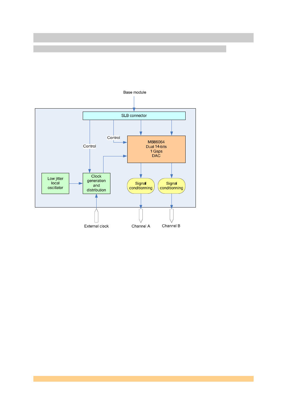
4 Functional Description
4.1 Block Diagram
The following diagram represents the architecture of the SMT381 daughter module.
Figure 1: block diagram of the SMT381
The SMT381 is a daughter board that plugs onto a base board.
The base board sends the digital samples for the DAC and control data for the on-board
clocks and the DAC via the SLB connector.
There are two DAC cores present in the MB86064. Thus two channels are available for
outputs. The outputs of the DAC are differential currents, which are converted to a
voltage by the analogue output stage (RF Transformer).
There are three sources for the sampling clock of the DAC
• the on-board VCO,
• the on-board Clock synthesizer,
• the external clock can be provided as an LVPECL clock or as an RF clock (two
separate inputs).
User Manual SMT381
Last Edited: 12/06/2007 10:43:00